
Method for judging open circuit defect of through hole

A defect and defect probability technology, applied in image data processing, instruments, calculations, etc., can solve problems such as the inability to determine the open circuit risk of process fluctuations

Pending Publication Date: 2022-03-01
NANJING CHENGXIN INTEGRATED CIRCUIT TECH RES INST CO LTD
View PDF0 Cites 0 Cited by
  • Summary
  • Abstract
  • Description
  • Claims
  • Application Information

AI Technical Summary

Problems solved by technology

[0013] The purpose of the present invention is to provide a method for judging the open circuit defect of a through hole, which aims to solve the problem that the existing technology can only determine whether the predetermined position is open circuit, but cannot determine the open circuit risk under process fluctuations

Method used


Image

  • Method for judging open circuit defect of through hole
  • Method for judging open circuit defect of through hole
  • Method for judging open circuit defect of through hole

Examples


Embodiment

[0071] S111 defines the step length of the metal profile, and differentiates the metal profile to obtain the area of ​​the metal profile;

[0072] The metal profile has a lot of vertices. In order to speed up calculation efficiency, the metal profile is differentiated / stepped, and the number of vertices of the metal profile is reduced, such as figure 1 .

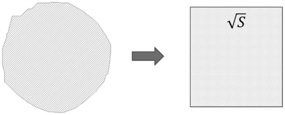
[0073] S112 calculates the outline area of ​​the through hole, and replaces the outline of the through hole with a square equal to the area of ​​the outline of the through hole;

[0074] calculating the area of ​​the through-hole outline by software, replacing the area of ​​the through-hole outline with a square with an equal area, and replacing the area of ​​the through-hole outline with the square, figure 2 The left side is the outline of the through hole, its area can be obtained by software calculation, and the area is recorded as S, figure 2 On the right is the area and figure 2 For a square with the same through-...


PUM


Abstract

The invention relates to the technical field of integrated circuits, in particular to a method for judging open circuit defects of through holes. Comprising the following steps: defining a metal contour step length, and differentiating a metal contour to obtain a metal contour area; calculating the contour area of the through hole, and replacing the contour of the through hole with a square with the same area as the contour of the through hole; calculating the overlapping area of the square and the metal contour; potential open circuit defect probabilities in the metal contour direction and the direction perpendicular to the metal contour direction are calculated based on the overlapping area, so that whether the open circuit of the through hole is defective or not is judged, overlay errors can cause that the through hole cannot accurately fall in a preset design position and finally fall in a certain range, and the defect probability of the open circuit is calculated to judge whether the open circuit of the through hole is defective or not. The problem that in the prior art, only whether an open circuit occurs at a preset position or not can be determined, and the open circuit risk under process fluctuation cannot be determined is solved.

Description

technical field [0001] The invention relates to the technical field of integrated circuits, in particular to a method for judging the open defect of a through hole. Background technique [0002] For the calculation and judgment of optical proximity effect correction, the main method includes the following steps: [0003] (1) Calculate the overlapping area of ​​the contour of the via after exposure / etching and the contour of the metal metal; [0004] (2) Calculate the ratio of the overlapping area to the area of ​​the original design size via, expressed as [0005] Area ratio = overlapping area / area of ​​original design size via [0006] (3) Calculate according to the process variation range, and finally set the safety threshold of the area ratio (threshold); [0007] (4) If the actual area ratio is higher than or equal to the safety threshold threshold: [0008] Area ratio ≥ safety threshold threshold [0009] The through hole via can be judged as no open circuit defe...

Claims


Application Information

Patent Timeline
IPC IPC(8): G06T7/00G06T7/62
CPCG06T7/0002G06T7/62G06T2207/30148
Inventor 苏晓菁韦亚一粟雅娟张利斌刘畅张世鑫
Owner NANJING CHENGXIN INTEGRATED CIRCUIT TECH RES INST CO LTD
Learn More