
Additives for Alkaline Polishing of Silicon Wafers and Their Applications

A silicon wafer alkali and additive technology, applied in water-based dispersants, sustainable manufacturing/processing, final product manufacturing, etc., to achieve pollution-free and controllable polishing, increase slurry tension, and gain battery conversion efficiency

Active Publication Date: 2022-06-07
CHANGZHOU SHICHUANG ENERGY CO LTD
View PDF8 Cites 0 Cited by
  • Summary
  • Abstract
  • Description
  • Claims
  • Application Information

AI Technical Summary

Problems solved by technology

At present, the additives for monocrystalline silicon back polishing on the market can only form larger-sized tower bases, and there is no additive that can form smaller-sized tower bases on the market.

Method used


Image

  • Additives for Alkaline Polishing of Silicon Wafers and Their Applications
  • Additives for Alkaline Polishing of Silicon Wafers and Their Applications
  • Additives for Alkaline Polishing of Silicon Wafers and Their Applications

Examples


Embodiment 1

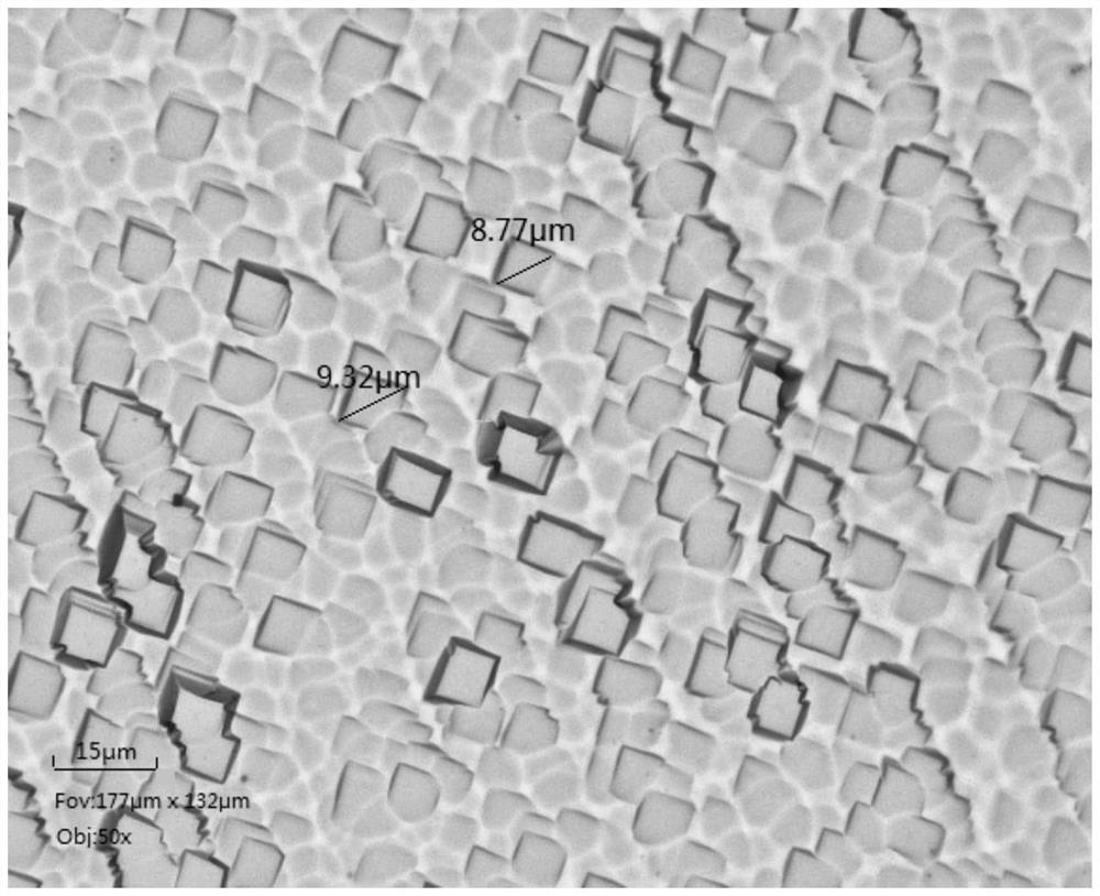
[0042] 1) Preparation of additives: 0.75 parts by mass of gelatin, 2 parts by mass of acrylamide, 0.5 parts by mass of benzyltriethylammonium chloride, 3 parts by mass of sodium p-aminosalicylate, 4 parts by mass of ammonium thiocyanate, 3 parts by mass of Alkyl glycosides and 0.2 parts by mass of sodium benzoate were added to 86.55 parts by mass of deionized water, and mixed uniformly to prepare additives;

[0043] 2) Preparation of polishing liquid: add the additive prepared in step 1) into the potassium hydroxide solution, and mix evenly to prepare a polishing liquid; the mass ratio of the additive to the potassium hydroxide solution is 1:100; The mass percentage of potassium is 3%;

[0044] 3) Alkali polishing: use the polishing liquid prepared in step 2) to polish the single crystal silicon wafer, and the temperature of the polishing treatment is controlled at 70° C. and the time is controlled at 180s.

[0045] Example 1 The scanning electron microscope image of the back...

Embodiment 2

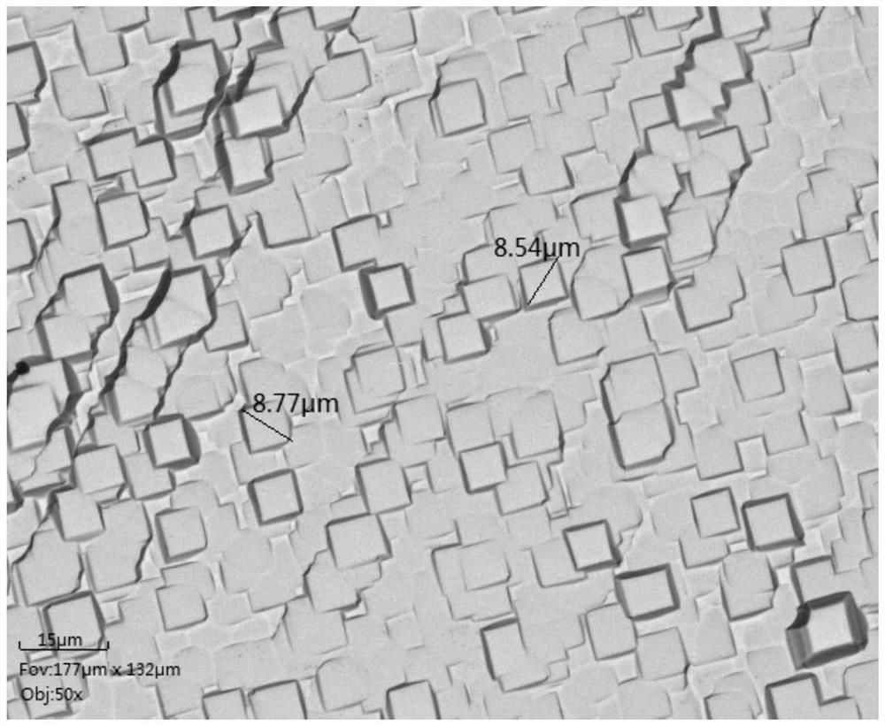
[0047] 1) Preparation of additives: 1.5 parts by mass of gelatin, 1.5 parts by mass of acrylamide, 1 part by mass of tetrabutylammonium chloride, 3 parts by mass of sodium p-aminosalicylate, 5 parts by mass of ammonium thiocyanate, 4 parts by mass of alkyl Glycosides and 0.2 parts by mass of sodium benzoate were added to 83.8 parts by mass of deionized water, and mixed evenly to prepare additives;

[0048] 2) Preparation of polishing liquid: Add the additive prepared in step 1) to the potassium hydroxide solution, and mix it evenly to prepare a polishing liquid; the mass ratio of the additive to the potassium hydroxide solution is 0.75:100; The mass percentage of potassium is 2.5%;

[0049] 3) Alkali polishing: use the polishing liquid prepared in step 2) to polish the single crystal silicon wafer, and the temperature of the polishing treatment is controlled at 60°C and the time is controlled at 240s).

[0050] Example 2 The scanning electron microscope image of the back of t...


PUM

PropertyMeasurementUnit
sizeaaaaaaaaaa
sizeaaaaaaaaaa

Abstract

The invention discloses an additive for alkali polishing of silicon wafers. The content of each component is: 0.5-2 parts by mass of gelatin, 1-2 parts by mass of acrylamide, 0.5-2 parts by mass of quaternary ammonium salt, 1-3 parts by mass of Sodium p-aminosalicylate, 4-5 parts by mass of ammonium thiocyanate, 3-4 parts by mass of alkyl glycoside, 0.1-0.3 parts by mass of sodium benzoate, and 81.7-89.9 parts by mass of water. Adding the additive of the present invention to the polishing liquid of silicon wafer alkali polishing can change the reaction rate of [111] / [100] plane, suppress the reaction speed of [100] plane, can change the flatness of the back side of silicon wafer, and can make alkali polishing A relatively rough small-sized tower-like structure is formed on the back of the silicon wafer, which slightly reduces the reflectivity of the back of the silicon wafer, which is conducive to the contact of the back paste, improves the pulling force of the paste, and can also improve the FF and improve the electrical performance of the cell.

Description

technical field [0001] The invention relates to the field of photovoltaics, in particular to an additive for alkali polishing of silicon wafers and its application. Background technique [0002] The additive for single crystal silicon back polishing refers to the chemical additives added in the polishing solution to help protect the front PN junction of the silicon wafer from being damaged and improve the back polishing effect during the manufacturing process of the single crystal silicon solar cell. In the production process of crystalline silicon solar cells, in order to further improve the performance and efficiency of the cells, the back of the silicon wafer is usually polished to make the back surface of the silicon wafer smoother or even achieve a mirror effect. On the one hand, the reflection of transmitted light can be strengthened to reduce the light transmittance, and on the other hand, the contact between the aluminum paste and the surface of the silicon wafer can...

Claims


Application Information

Patent Timeline
Patent Type & Authority Patents(China)
IPC IPC(8): C30B33/10
CPCC09G1/04H01L21/30604Y02P70/50
Inventor 裴银强章圆圆陈培良
Owner CHANGZHOU SHICHUANG ENERGY CO LTD
Learn More