
LED and IC high-density integrated packaging structure and process and LED lamp strip

An integrated packaging, high-density technology, applied in the direction of lighting devices, lighting and heating equipment, components of lighting devices, etc., can solve the problems of large spacing between components, low degree of integration, poor light-gathering performance, etc., to simplify the process , reduce the amount of materials, the effect of high output

Pending Publication Date: 2022-02-08
HEFEI SMAT TECH CO LTD
View PDF0 Cites 1 Cited by
  • Summary
  • Abstract
  • Description
  • Claims
  • Application Information

AI Technical Summary

Problems solved by technology

[0002] The traditional LED chip packaging is wire bonding, and the IC chip is also wire bonding. After the IC chip and the LED chip are all attached to the LED strip, the IC chip and the LED chip are connected through a conductive device or a wire, and then sealed with glue for light transmission. , the structure made by this process will lead to large spacing between components and low integration degree when laying out components, which will lead to large packaging volume and poor light-gathering performance

Method used


Image

  • LED and IC high-density integrated packaging structure and process and LED lamp strip
  • LED and IC high-density integrated packaging structure and process and LED lamp strip
  • LED and IC high-density integrated packaging structure and process and LED lamp strip

Examples


Embodiment Construction

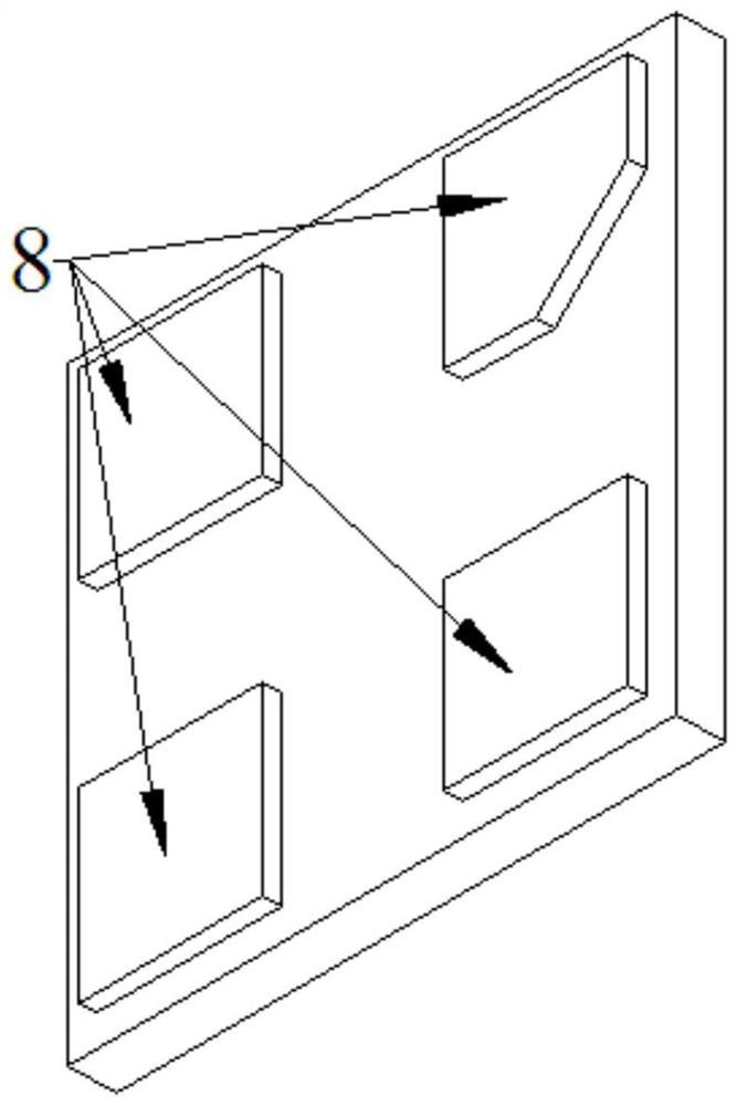
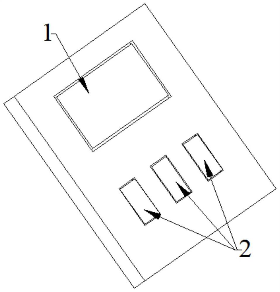
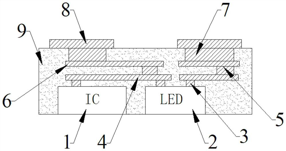
[0038] In order to better understand the purpose, structure and function of the present invention, below in conjunction with appendix Figure 1-9 , to further describe in detail the LED chip and IC high-density integrated package structure, process and LED light strip of the present invention.

[0039] LED chips have light-emitting properties, such as Figure 8 For the traditional LED chip control shown in the figure, after pasting IC chip 1, LED chip 2 or their packages on the LED strip, connect IC chip 1 and LED chip 2 through conductive devices or wires, and then seal them with glue. For light transmission, this method of glue and wire bonding will lead to large spacing between components and low degree of integration when arranging components, resulting in large packaging volume, many materials, and high cost.

[0040] Such as image 3 , design LED and IC high-density integrated packaging structure, including IC chip 1, LED chip 2 and packaging layer 9; wherein, the stru...


PUM


Abstract

The invention discloses an LED and IC high-density integrated packaging structure and process and an LED lamp strip. The packaging structure comprises an IC chip and an LED chip, and the IC chip and the LED chip are electrically connected. The packaging structure further comprises a packaging layer, the IC chip and the LED chip are packaged in the packaging layer in an injection molding packaging mode, and the passive face of the IC chip and the front light-emitting face of the LED chip both face the same free face. The packaging structure further comprises an external terminal arranged on the outer wall surface of the packaging layer, and the external terminal is electrically connected with the IC chip. The LED and IC high-density integrated packaging structure and process and the LED lamp strip have the following advantages that high-density integration is achieved, the packaging size is reduced, the packaging structure is lighter and thinner, the cost is lower, various light-emitting units and control ICs can be integrated, and the packaging structure is particularly suitable for wearable equipment of consumers.

Description

technical field [0001] The invention belongs to the technical field of semiconductor packaging, and in particular relates to a LED and IC high-density integrated packaging structure, process and LED light strip. Background technique [0002] The traditional LED chip packaging is wire bonding, and the IC chip is also wire bonding. After the IC chip and the LED chip are all attached to the LED strip, the IC chip and the LED chip are connected through a conductive device or a wire, and then sealed with glue for light transmission. , The structure made by this process, when laying out components, will lead to large spacing between components, low degree of integration, resulting in large packaging volume and poor light-gathering performance. To this end, LED and IC high-density integrated packaging structure, technology and LED light strip are proposed. Contents of the invention [0003] In order to solve the above-mentioned problems in the prior art, the present invention pr...

Claims


Application Information

Patent Timeline
IPC IPC(8): H01L25/16H01L33/48F21V19/00F21V23/06F21Y115/10
CPCH01L25/167H01L33/486F21V19/001F21V23/06F21Y2115/10H01L2933/0033
Inventor 张光耀谭小春
Owner HEFEI SMAT TECH CO LTD
Learn More