High-reliability MOSFET integrated circuit chip and preparation method thereof

An integrated circuit and reliability technology, which is applied in the field of high-reliability MOSFET integrated circuit chips and their preparation, can solve the problems of weak withstand voltage in the terminal area, burn the transition area attachment, and fail to pass the reliability, so as to improve device performance, The effect of smoothing electric field lines and improving reliability

Pending Publication Date: 2022-01-18
捷捷微电(无锡)科技有限公司
View PDF6 Cites 0 Cited by
  • Summary
  • Abstract
  • Description
  • Claims
  • Application Information

AI Technical Summary

Problems solved by technology

This structure can still be used in low-voltage products (30-100V), but when the voltage reaches 120V or more, it will encounter the problem of weak avalanche capability and unreliable reliability, and usually burns the accessories in the transition zone
The analysis found that the fundamental reason is that the terminal area formed solely by 1-3 deep grooves has a weak withstand voltage capability

Method used


Image

  • High-reliability MOSFET integrated circuit chip and preparation method thereof

Examples


Embodiment Construction

[0031] In order to make the purposes, technical solutions and advantages of the embodiments of the present application clearer, the technical solutions in the embodiments of the present application will be clearly and completely described below in conjunction with the drawings in the embodiments of the present application. Obviously, the described embodiments It is a part of the embodiments of this application, not all of them. Based on the embodiments in this application, all other embodiments obtained by persons of ordinary skill in the art without making creative efforts belong to the scope of protection of this application.

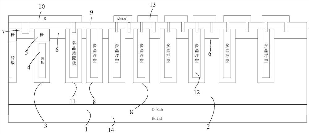
[0032] The invention provides a high-reliability MOSFET integrated circuit chip and a preparation method thereof. By increasing the number of the second-type trenches in the termination region and increasing the width of the platform region (mesa) between the second-type trenches, the withstand voltage capability and reliability of the MOSFET terminat...


PUM


Abstract

The invention discloses a high-reliability MOSFET integrated circuit chip and a preparation method thereof. The high-reliability MOSFET integrated circuit chip comprises a terminal area. At least one first-type groove (11) and at least two second-type grooves (8) are arranged in the terminal area; source electrode conductive polycrystalline silicon (4) is arranged in the first type of grooves (11); floating polycrystalline silicon (12) is arranged in the second type of grooves (8); and the number of the first type of grooves (11) and the number of the second type of grooves (8) are increased to improve the voltage endurance capability of the terminal area, and the width of the platform area adjacent to the second type of grooves (8) is gradually increased.

Description

technical field [0001] The invention relates to the field of semiconductor integrated circuit chip manufacturing, in particular to a highly reliable MOSFET integrated circuit chip and a preparation method thereof. Background technique [0002] A MOSFET integrated circuit chip usually has a deep trench structure. The inside of the trench is divided into a top gate and a bottom gate. There is an isolation oxide layer in the middle. There are thinner oxide layers on both sides of the top gate as the gate oxide layer, and thinner oxide layers on both sides of the bottom gate. The thick oxide layer acts as a field oxide. This MOSFET device has extremely low conduction loss and extremely low switching loss, and allows higher current density in a smaller package, which can meet the requirements of space saving and high efficiency in applications, so it is used in fast charging , electric vehicles, automotive electronics and other high-end fields are more and more widely used. [...

Claims


Application Information

Patent Timeline
Patent Type & Authority Applications(China)
IPC IPC(8): H01L29/78H01L29/06H01L29/40H01L21/336
CPCH01L29/7813H01L29/0619H01L29/407H01L29/66734
Inventor 刘秀梅刘锋殷允超周祥瑞
Owner 捷捷微电(无锡)科技有限公司
Why Eureka
Try Eureka