
Avalanche photodiode device with curved absorption region

A technology of avalanche optoelectronics and absorption regions, which is applied in the direction of electrical components, semiconductor devices, circuits, etc., can solve the problems of complex epitaxy and difficulty in integration, and achieve the effect of uniform electric field distribution

Pending Publication Date: 2022-01-14
INTERUNIVERSITAIR MICRO ELECTRONICS CENT (IMEC VZW)
View PDF0 Cites 0 Cited by
  • Summary
  • Abstract
  • Description
  • Claims
  • Application Information

AI Technical Summary

Problems solved by technology

This vertical SACM APD device with a dedicated epitaxial growth stack is difficult to integrate into existing silicon photonics platforms due to epitaxial complexity

Method used


Image

  • Avalanche photodiode device with curved absorption region
  • Avalanche photodiode device with curved absorption region
  • Avalanche photodiode device with curved absorption region

Examples


Embodiment Construction

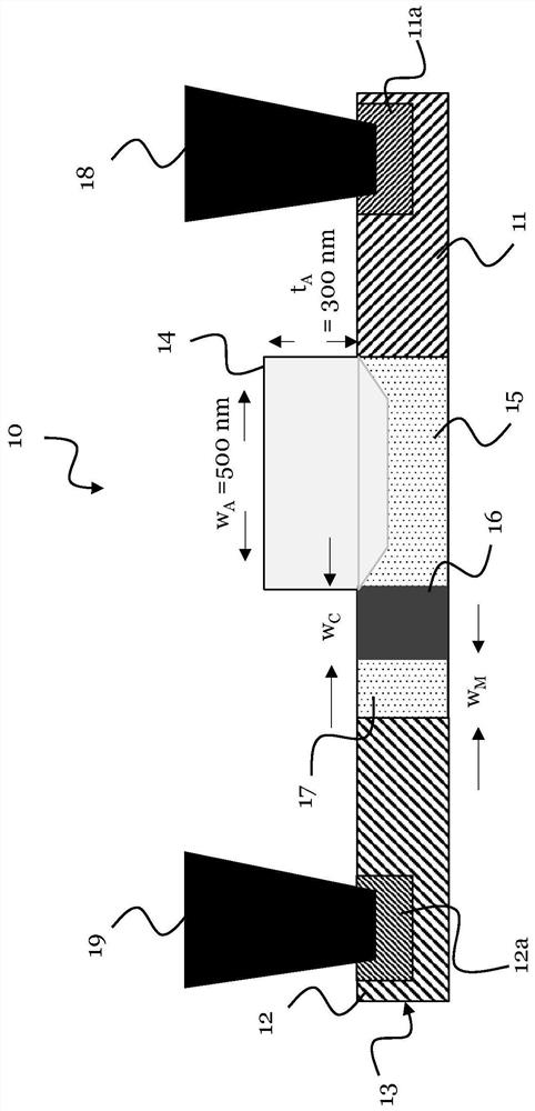
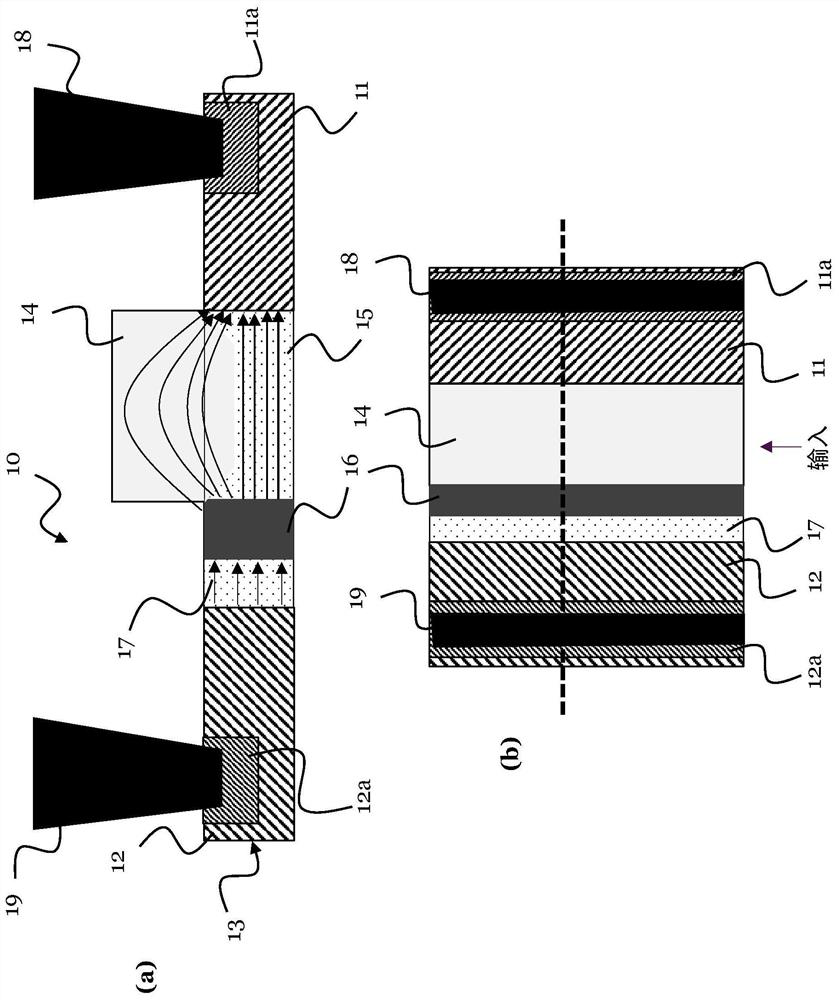
[0053] Figure 4 An APD device 40 according to an embodiment of the invention is shown. in particular, Figure 4 (b) shows a top view of the APD device 40, Figure 4 (a) shows the APD device 40 along Figure 4 Cross-section of dashed line in (b).

[0054] The APD device 40 includes a first contact region 41 and a second contact region 42 formed in a semiconductor layer 43 . The semiconductor layer 43 may be a silicon layer, for example may be the top layer of a silicon-on-insulator (SOI) substrate. The first contact region 41 may be a p-type doped region, and the second contact region 42 may be an n-type doped region.

[0055] The APD device 40 further comprises an absorption region 44 formed on the semiconductor layer 43, wherein the absorption region 44 is at least partially formed on a first region 45 of the semiconductor layer 43, wherein the first region 45 is arranged at the first contact region 41 and the second contact area 42. The first region 45 may be an intr...


PUM

PropertyMeasurementUnit
widthaaaaaaaaaa

Abstract

The present disclosure proposes an avalanche photodiode (APD) device, in particular, a lateral separate absorption charge multiplication (SACM) APD device, and a method for its fabrication. The APD device comprises a first contact region and a second contact region formed in a semiconductor layer. Further, it comprises an absorption region formed on the semiconductor layer, wherein the absorption region is at least partly formed on a first region of the semiconductor layer, wherein the first region is arranged between the first contact region and the second contact region. The APD device further includes a charge region formed in the semiconductor layer between the first region and the second contact region, and an amplification region formed in the semiconductor layer between the charge region and the second contact region. At least the absorption region is curved on the semiconductor layer.

Description

technical field [0001] The present disclosure relates to photodetectors, in particular avalanche photodetectors, and is directed to applications for optical communications, light sensing or quantum communications. The present disclosure proposes an avalanche photodiode (APD) device, in particular, a split absorbing charge multiplying (SACM) APD device, and a method for fabricating the APD device. The APD device proposed in this disclosure may be a lateral SACM APD device with a curved absorbing region. Background technique [0002] In the technical field of APD devices given above (e.g., used as photodetectors for optical communication, light sensing or quantum communication), receiver sensitivity and operating data rate are key performance requirements, because they determine the optical communication chain power consumption of the road. APD devices have great potential to meet these requirements and thus realize sensitive receivers allowing high operating data rates. ...

Claims


Application Information

Patent Timeline
Patent Type & Authority Applications(China)
IPC IPC(8): H01L31/107H01L31/18
CPCH01L31/107H01L31/18H01L31/1075H01L31/028H01L31/02327H01L31/035281H01L31/03529H01L31/1808
Inventor A·斯里尼瓦桑M·I·潘图瓦基J·范卡姆潘豪特
Owner INTERUNIVERSITAIR MICRO ELECTRONICS CENT (IMEC VZW)
Learn More