Liquid crystal micro-optical structure and liquid crystal-based electric dimming light field imaging detection chip

A photodetector and micro-optics technology, applied in optics, nonlinear optics, instruments, etc., can solve the problem of low depth of field expansion ability and achieve clear imaging effect

Pending Publication Date: 2021-12-24
HUAZHONG UNIV OF SCI & TECH
View PDF0 Cites 0 Cited by
  • Summary
  • Abstract
  • Description
  • Claims
  • Application Information

AI Technical Summary

Problems solved by technology

However, the existing liquid crystal microlens can only achieve one focal length in one optical imaging process, and the ability to expand the depth of field is relatively low.

Method used


Image

  • Liquid crystal micro-optical structure and liquid crystal-based electric dimming light field imaging detection chip
  • Liquid crystal micro-optical structure and liquid crystal-based electric dimming light field imaging detection chip
  • Liquid crystal micro-optical structure and liquid crystal-based electric dimming light field imaging detection chip

Examples


Embodiment Construction

[0021] In order to make the object, technical solution and advantages of the present invention clearer, the present invention will be further described in detail below in conjunction with the accompanying drawings and embodiments. It should be understood that the specific embodiments described here are only used to explain the present invention, not to limit the present invention. In addition, the technical features involved in the various embodiments of the present invention described below can be combined with each other as long as they do not constitute a conflict with each other.

[0022] In the present invention, the terms "first", "second" and the like (if any) in the present invention and drawings are used to distinguish similar objects, and are not necessarily used to describe a specific order or sequence.

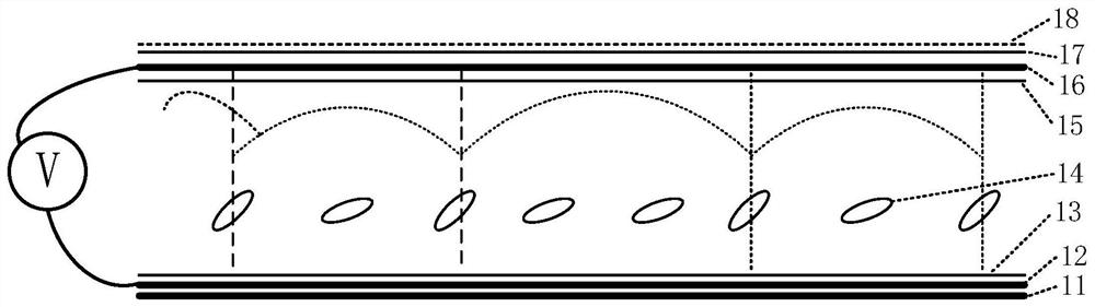
[0023] figure 1 Schematic diagram of the structure of the liquid crystal micro-optical structure provided by the embodiment of the present invention. refer to f...


PUM


Abstract

The invention discloses a liquid crystal micro-optical structure and a liquid crystal-based electric dimming light field imaging detection chip, and belongs to the field of optical imaging detection. The liquid crystal micro-optical structure comprises a liquid crystal material layer, and a patterned electrode layer and a common electrode layer which are respectively arranged on the two sides of the liquid crystal material layer. The patterned electrode layer is composed of a conductive film, electrode micropores distributed in an array are formed in the conductive film, the electrode micropores with different apertures are alternately arranged, and the electrode micropores with the same aperture are periodically arranged. When the mean square amplitude of a signal voltage applied between the patterned electrode layer and the common electrode layer is higher than a mean square amplitude threshold, liquid crystal molecules in the liquid crystal material layer under the electrode micropores with different apertures are in different spatial arrangement forms, so that gradient refractive index distribution corresponding to the periodic alternating array distribution is formed in the liquid crystal material layer, and the liquid crystal micro-optical structure has a plurality of focal lengths at the same moment. The multiple focal lengths can expand the field depth range for the second time, so that objects in a wider depth range in a view field can be clearly imaged.

Description

technical field [0001] The invention belongs to the field of optical imaging detection, and more specifically relates to a liquid crystal micro-optical structure and a liquid crystal-based electric modulation light field imaging detection chip. Background technique [0002] As an emerging imaging modality, light field imaging technology has triggered a new wave of research and entered the consumer market in 2012. Conventional imaging methods use the main lens to project the 3D scene onto the 2D detector plane, which directly causes the loss of the original depth information. Light field imaging can obtain four-dimensional space and angle information of a three-dimensional object space scene by adding a layer of microlens arrays between the main lens and the detector. Light field imaging has the unique advantage of "shooting first, focusing later", and can realize multiple imaging applications such as multi-view imaging, digital refocusing, full-focus imaging, depth estimati...

Claims


Application Information

Patent Timeline
Patent Type & Authority Applications(China)
IPC IPC(8): G02F1/1343G02F1/1337G02F1/133G02F1/13
CPCG02F1/134309G02F1/134318G02F1/1337G02F1/1313G02F1/13306
Inventor 陈明策刘可薇王哲张新宇
Owner HUAZHONG UNIV OF SCI & TECH
Why Eureka
Try Eureka