Shield gate trench MOSFET manufacturing method

A manufacturing method and shielding grid technology, applied in semiconductor/solid-state device manufacturing, semiconductor devices, electrical components, etc., to achieve the effects of reducing production costs, wide use, and shortening processing time

Active Publication Date: 2021-12-03
深圳利普芯微电子有限公司
View PDF7 Cites 1 Cited by
  • Summary
  • Abstract
  • Description
  • Claims
  • Application Information

AI Technical Summary

Problems solved by technology

[0009] The purpose of this application is to overcome the deficiencies of the prior art and provide a method for manufacturing a shielded gate trench MOSFET, which can solve many defects in the existing shielded gate trench MOSFET isolation technology

Method used


Image

  • Shield gate trench MOSFET manufacturing method
  • Shield gate trench MOSFET manufacturing method
  • Shield gate trench MOSFET manufacturing method

Examples


Embodiment Construction

[0053] The technical solution of the present application will be further described in detail below in conjunction with specific embodiments, but the protection scope of the present application is not limited to the following description.

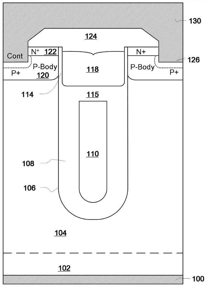
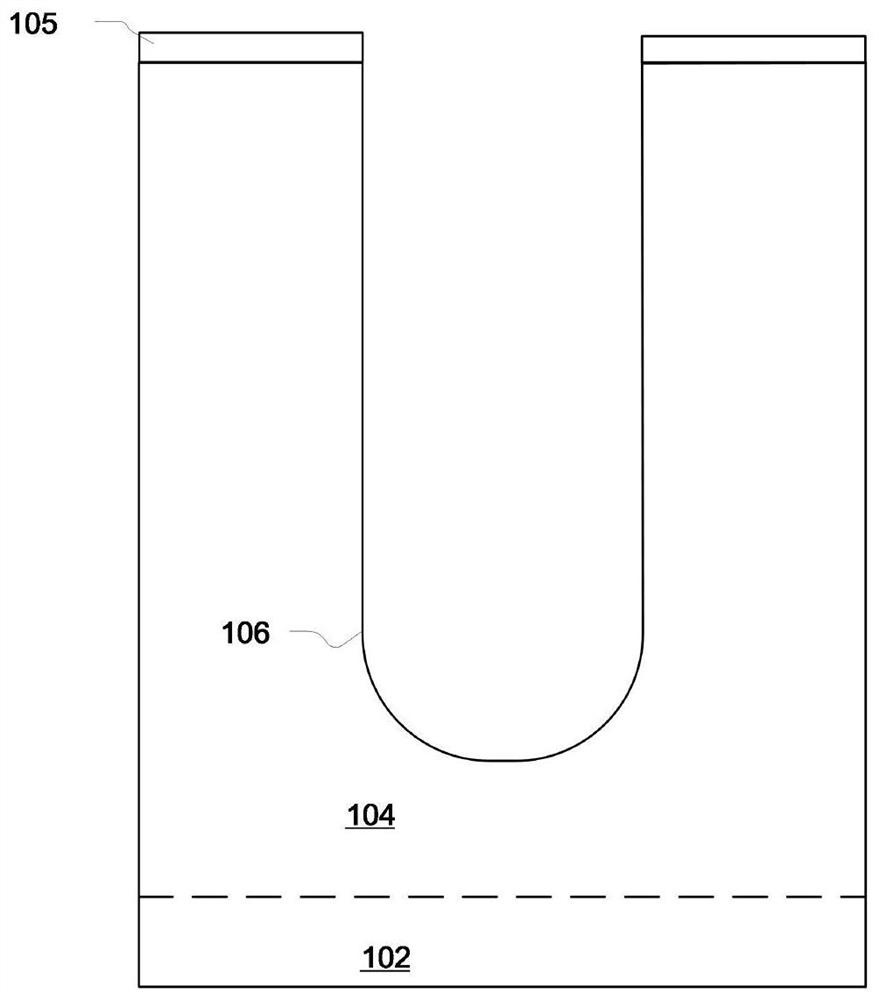
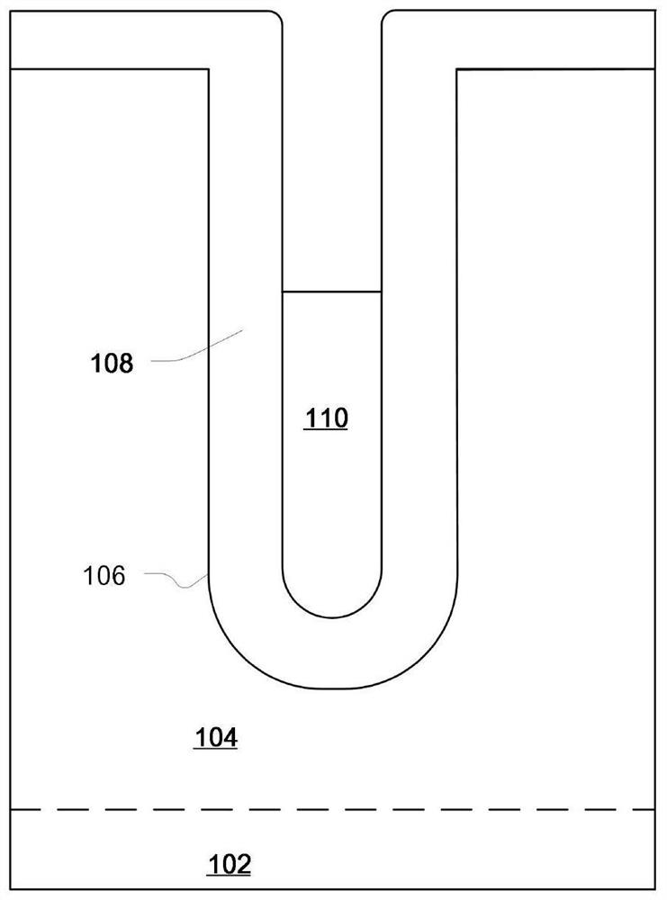
[0054] In some embodiments, a shielded gate trench MOSFET manufacturing method comprises growing a shielded gate oxide layer 108 on the sidewall of the trench 106 of the epitaxial layer 104, then filling the shielded gate polysilicon 110, and etching the shielded gate polysilicon 110 back to the first target depth;

[0055] Depositing a silicon nitride layer 112 with a target thickness T to form a dielectric isolation layer isolating the shielding gate polysilicon 110 and the gate polysilicon 118, and etching the silicon nitride layer 112 back to the surface of the epitaxial layer;

[0056] Etch the shielding gate oxide layer 108 to the second target depth, etch the silicon nitride layer 112 to the first target thickness K, so that the upper...


PUM


Abstract

The invention relates to a shield gate trench MOSFET manufacturing method, which comprises the following steps: growing a shield gate oxide layer on the side wall of a trench of an epitaxial layer, then conducting filling with shield gate polycrystalline silicon, and etching back the shield gate polycrystalline silicon to a first target depth; depositing a silicon nitride layer with a target thickness T to form a dielectric isolation layer for isolating the shield gate polycrystalline silicon and the device gate, and etching the silicon nitride layer back to the surface of the epitaxial layer; etching the shield gate oxide layer to a second target depth, and etching the silicon nitride layer to a first target thickness K, so as to enable the upper surface of the silicon nitride layer to extend out of the surface of the shield gate oxide layer; and growing a gate oxide layer, depositing gate polycrystalline silicon, and etching the gate polycrystalline silicon to a third target depth to form the shield gate trench MOSFET. The shield gate trench MOSFET and the manufacturing method thereof have the advantages of stable structure, high production efficiency, low cost and the like.

Description

technical field [0001] The present application relates to the field of manufacturing shielded gate trench MOSFETs, in particular to a method for manufacturing shielded gate trench MOSFETs. Background technique [0002] Shielded gate trench MOSFET is currently the most advanced power MOSFET device technology, which has the advantages of lower on-resistance and faster switching speed than traditional trench MOSFET. In system applications, it has lower conduction loss and lower switching loss, and the system has higher conversion and transmission efficiency. figure 1 It is a schematic diagram of the shielded gate trench MOSFET cell structure; in order to obtain the above advantages, such as figure 1 As shown, the shielded gate trench MOSFET introduces a shielded gate structure, and the shielded gate polysilicon 110 is isolated from the gate of the device through an insulating dielectric layer. The process of isolating the shielded gate polysilicon 110 from the device gate is ...

Claims


Application Information

Patent Timeline
IPC IPC(8): H01L29/78H01L29/423H01L29/06H01L21/336
CPCH01L29/78H01L29/0603H01L29/0684H01L29/4236H01L29/66477H01L29/7813H01L29/407H01L29/66734H01L29/41766
Inventor 孙健其他发明人请求不公开姓名
Owner 深圳利普芯微电子有限公司
Why Eureka
Try Eureka