Tower-type PCB and stitching method thereof

A PCB board and tower type technology, applied in the field of tower type PCB boards and their stitching, can solve the problems of failure to improve the pass rate, inconvenient welding operation of tower type circuit boards, high production costs, etc., and achieve small mechanical damage , The solder paste is evenly distributed and the deformation is small

Pending Publication Date: 2021-11-30
雅安小航电器股份有限公司
View PDF0 Cites 2 Cited by
  • Summary
  • Abstract
  • Description
  • Claims
  • Application Information

AI Technical Summary

Problems solved by technology

[0016] The technical problem to be solved by the present invention is that the welding operation of the tower type circuit board is inconvenient at present, the production cost remains high, and the pass rate cannot be improved. The purpose is to provide a tower type PCB board and its sewing method. By adopting this scheme, Ensure the effective stitching of the PCB board, avoid the deformation and dislocation of the upper and lower PCB boards, and at the same time satisfy the penetration of solder from the stitching hole to the other side of the PCB board, ensuring that the other side is welded without missing soldering, virtual soldering, surfacing, etc. unpleasant sight

Method used


Image

  • Tower-type PCB and stitching method thereof
  • Tower-type PCB and stitching method thereof
  • Tower-type PCB and stitching method thereof

Examples


Embodiment 1

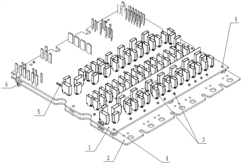
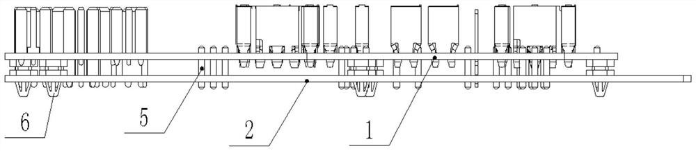
[0045] This embodiment provides a tower PCB board, such as Figure 1-Figure 3 As shown, it includes the PCB board body, the PCB board body includes the upper board 1 and the lower board 2, and also includes the guideline 5;

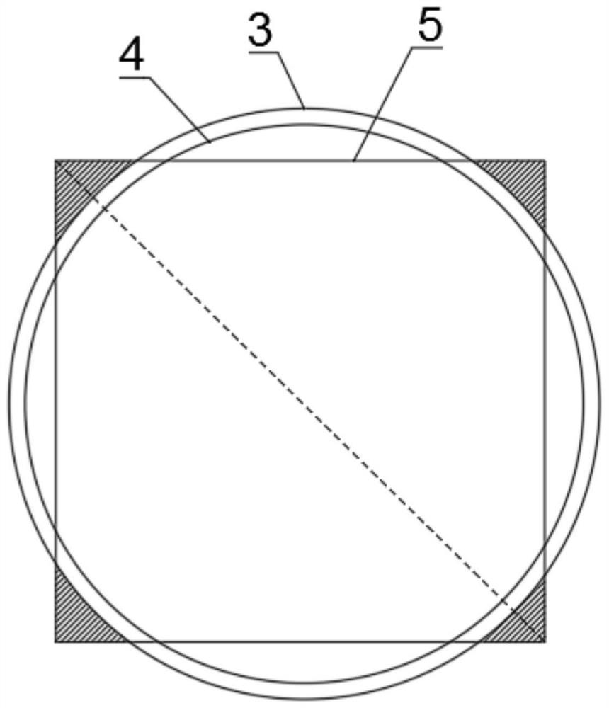
[0046] The PCB board body is provided with a plurality of welding stitching holes 3 and fixing stitching holes 4, and the guideline 5 can be inserted into the welding stitching holes 3 and the fixing stitching holes 4 and stitched for fixing the upper board 1 and the lower board 2. The welding suture hole and the fixed suture hole are all matched with the guideline gap, and the cross-sectional diagonal length of the guideline is greater than the aperture of the welded suture hole and the fixed suture hole, and the aperture of the fixed suture hole is smaller than that of the welded suture hole aperture.

[0047] Compared with the existing technology, the soldering operation of the tower circuit board is inconvenient, the production cost remains high, and t...

Embodiment 2

[0053] This embodiment is further optimized on the basis of Embodiment 1, and a method for sewing tower PCB boards is provided, including the following steps:

[0054] Step 1: evenly distribute the solder paste on the pads on the upper surface of the upper board 1 and the lower board 2;

[0055] The second step: overlap the upper plate 1 and the lower plate 2 towers;

[0056] Step 3: After overlapping, insert guideline 5 into fixed suture hole 4 for suture;

[0057] Step 4: Then insert guideline 5 into welding suture hole 3 to suture;

[0058] Step 5: Use reflow soldering to solder the PCB board body to complete the fixing of the PCB board body.

[0059] In this embodiment, the fronts of the upper board 1 and the lower board 2 are printed with solder paste, and the solder paste is evenly distributed on the welding pads of the welding seam holes 3 and the fixed seam holes 4; At the suture position, the solder paste can be evenly distributed.

[0060] In this embodiment, the...

Embodiment 3

[0065] This embodiment is further optimized on the basis of embodiment 2, and a specific implementation manner is provided.

[0066] Process before sewing:

[0067] Firstly, it is printed by a printing machine, and the solder paste is evenly distributed on the pads of the front stitching holes of the PCB board. The thickness of the solder paste is 0.5mm; the PCB board plug-in and patch are completed, and the overlapping combination of the upper and lower PCB boards is completed and fixed. , to be sutured later.

[0068] Stitching process:

[0069] The first step: First, stack the PCB boards and keep the overlapping position of the tower PCB boards fixed. This is a prerequisite for ensuring the effective stitching of the tower PCB boards in addition to the requirements for the size and accuracy of the PCB boards.

[0070] Step 2: Inserting the suture needle, manual or sewing machine insertion needle 5, should follow the following:

[0071] Material: 1.5*1.5mm guideline 5, th...


PUM


Abstract

The invention discloses a tower-type PCB and a stitching method thereof, which relate to the field of printed circuit boards. The tower-type PCB comprises a PCB body, the PCB body comprises an upper layer board and a lower layer board, and the PCB body also comprises square needles; the PCB body is provided with a plurality of welding stitching holes and fixing stitching holes, square needles can be inserted into the welding stitching holes and the fixing stitching holes for stitching, and the welding stitching holes and the fixing stitching holes are used for fixing an upper layer board and a lower layer board. The welding stitching hole and the fixing stitching hole are both in clearance fit with the square needle, the diagonal length of the cross section of the square needle is larger than the aperture of the welding stitching hole and the aperture of the fixing stitching hole, and the aperture of the fixing stitching hole is smaller than that of the welding stitching hole. By the adoption of the scheme, effective stitching of the PCBs can be guaranteed, the bad conditions of deformation, dislocation and the like of the upper PCB and the lower PCB are avoided, meanwhile, soldering tin can permeate to the other sides of the PCBs from the stitching holes, and it is guaranteed that welding on the other sides is free of the bad phenomena of solder skips, pseudo soldering, surfacing and the like.

Description

technical field [0001] The invention relates to the field of printed circuit boards, in particular to a tower type PCB board and a sewing method thereof. Background technique [0002] With the rapid development of the electronics industry, the tower circuit board has been widely used in the manufacturing industry due to its advantages such as small footprint. At present, domestic PCB boards have gradually become standardized. At present, the quality of tower circuit boards is mainly limited by the stitching process. How to achieve effective stitching of circuit boards has become the key to ensuring the quality of tower circuit boards. [0003] The traditional circuit board stitching is to stack the welded upper and lower circuit boards together with the help of tooling, and then insert the sewing needle into the stitching hole of the circuit board, such as manual soldering, dip soldering or wave soldering. [0004] However, this approach has many disadvantages: [0005] Th...

Claims


Application Information

Patent Timeline
Patent Type & Authority Applications(China)
IPC IPC(8): H05K1/14H05K3/36
Inventor 敖德彬韩梦鑫李瑞刘鹏李治陈玉彬张腾蛟杨克成王聪
Owner 雅安小航电器股份有限公司
Why Eureka
Try Eureka