Two-dimensional lattice multi-beam phased array and its design method

A two-dimensional lattice and design method technology, applied in radio wave measurement systems, laser parts, instruments, etc., can solve the problems of proportional increase in size, proportional increase in insertion loss, and complex distribution network of power dividers. Achieve the effect of reducing size, reducing interference, and small size

Active Publication Date: 2022-03-11
ZHEJIANG CHENGCHANG TECH
View PDF9 Cites 0 Cited by
  • Summary
  • Abstract
  • Description
  • Claims
  • Application Information

AI Technical Summary

Problems solved by technology

[0004] The technical problem to be solved by the present invention is that the distribution network of the power splitter will become extremely complicated with the increase of beams in the traditional multi-beam phased array, and the size will increase proportionally, resulting in the size of the power distribution synthesis network gradually exceeding the beam width phase control unit, and the insertion loss increases proportionally

Method used


Image

  • Two-dimensional lattice multi-beam phased array and its design method
  • Two-dimensional lattice multi-beam phased array and its design method
  • Two-dimensional lattice multi-beam phased array and its design method

Examples


Embodiment 1

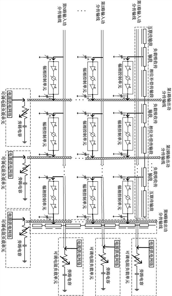
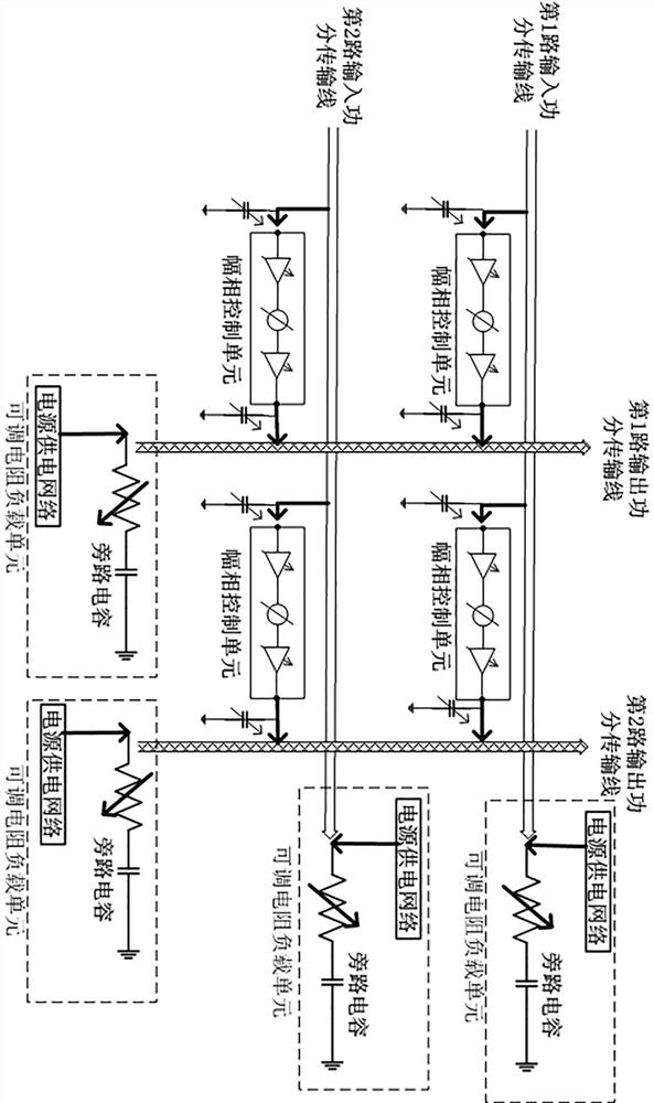
[0039] In order to solve the above technical problems existing in the prior art, an embodiment of the present invention provides a two-dimensional lattice multi-beam phased array.

[0040] figure 1 A schematic structural diagram of a two-dimensional lattice multi-beam phased array according to Embodiment 1 of the present invention is shown; refer to figure 1 As shown, the two-dimensional lattice multi-beam phased array in the embodiment of the present invention includes multiple parallel input power division transmission lines, multiple parallel output power division transmission lines, multiple amplitude and phase control units, and multiple adjustable resistance load units. .

[0041] Wherein, multiple parallel input power division transmission lines and multiple parallel output power division transmission lines are alternately arranged to form a power distribution network. Each input power division transmission line can be divided into multiple input lines, and each input...

Embodiment 2

[0050] In order to solve the above technical problems existing in the prior art, an embodiment of the present invention provides a two-dimensional lattice multi-beam phased array.

[0051] Image 6 A schematic flowchart of a method for designing a two-dimensional lattice multi-beam phased array according to Embodiment 2 of the present invention is shown. The two-dimensional lattice multi-beam phased array structure in this embodiment is the two-dimensional lattice multi-beam phased array provided in the first embodiment. Referring to FIG. 6 , the two-dimensional lattice in the embodiment of the present invention The multi-beam phased array design method is as follows.

[0052] Step S201, determining a preset impedance value of a transmission line with a preset structure.

[0053] First, the preset impedance value Z needs to be determined 0 , as the design basis for the characteristic impedance of all transmission sections. Further, the preset impedance value Z 0 The desig...


PUM


Abstract

The invention discloses a two-dimensional dot matrix multi-beam phased array and a design method thereof, wherein the two-dimensional dot matrix multi-beam phased array includes: multi-channel parallel input power division transmission lines, multi-channel parallel output power division Transmission lines, multiple amplitude and phase control units and multiple adjustable resistance load units, multiple parallel input power distribution transmission lines and multiple parallel output power distribution transmission lines are arranged alternately, and each input power distribution transmission line divides multiple input lines , each input line is respectively connected to an amplitude-phase control unit, each output power division transmission line is divided into multiple output lines, and each output line is connected to an amplitude-phase control unit, each input power division transmission line output terminal and each The input terminals of the output power division transmission line are respectively connected with an adjustable resistance load unit. The invention provides a two-dimensional dot matrix multi-beam phased array with small size and simple structure, which effectively improves the integration degree of multi-beam phased array chip design, reduces cost and is widely used.

Description

technical field [0001] The invention relates to the technical field of semiconductors, in particular to a two-dimensional lattice multi-beam phased array and a design method thereof. Background technique [0002] With the continuous development of phased array radar, people's demand for antenna wave speed control continues to increase, and the research on control circuits is also more in-depth. The multi-beam phased array radar can quickly scan and detect the airspace by forming multiple beams at the same time, and can also effectively track multiple fast-moving targets, which is a major advantage of the phased array radar. The traditional multi-beam phased array mainly realizes the distribution of signals through the power dividers of the Wilkinson structure and the size related to the electrical length. More crossovers become extremely complex and proportionally increase in size, which causes the power distribution and combining network to gradually exceed the size of the...

Claims


Application Information

Patent Timeline
Patent Type & Authority Patents(China)
IPC IPC(8): H01S5/00G01S7/02
CPCH01S5/00G01S7/02
Inventor 周甲武郑骎刘利平
Owner ZHEJIANG CHENGCHANG TECH
Why Eureka
Try Eureka