Display panel

A display panel, one-to-one corresponding technology, applied in the direction of semiconductor devices, electrical components, circuits, etc., can solve the problems of easy sliding and scratching of the spacer support column, avoid failure or abnormal display, and reduce the probability of fine particles. Effect

Active Publication Date: 2021-10-22
WUHAN CHINA STAR OPTOELECTRONICS SEMICON DISPLAY TECH CO LTD
View PDF5 Cites 0 Cited by
  • Summary
  • Abstract
  • Description
  • Claims
  • Application Information

AI Technical Summary

Problems solved by technology

[0004] The embodiment of the present application provides a display panel to solve the technical problem that the spacer support column of the existing display panel is easy to slide into the opening of the mask and be scratched

Method used


Image

  • Display panel
  • Display panel
  • Display panel

Examples


Embodiment Construction

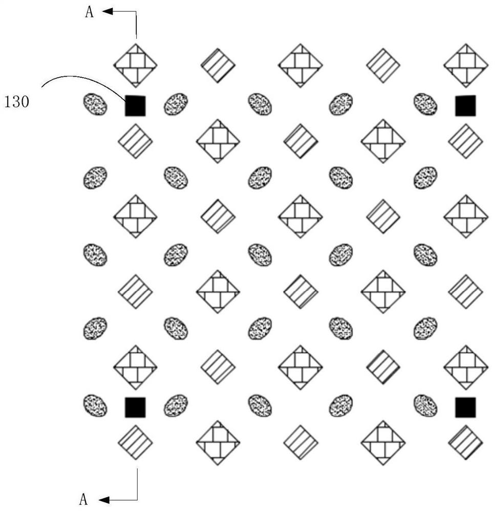
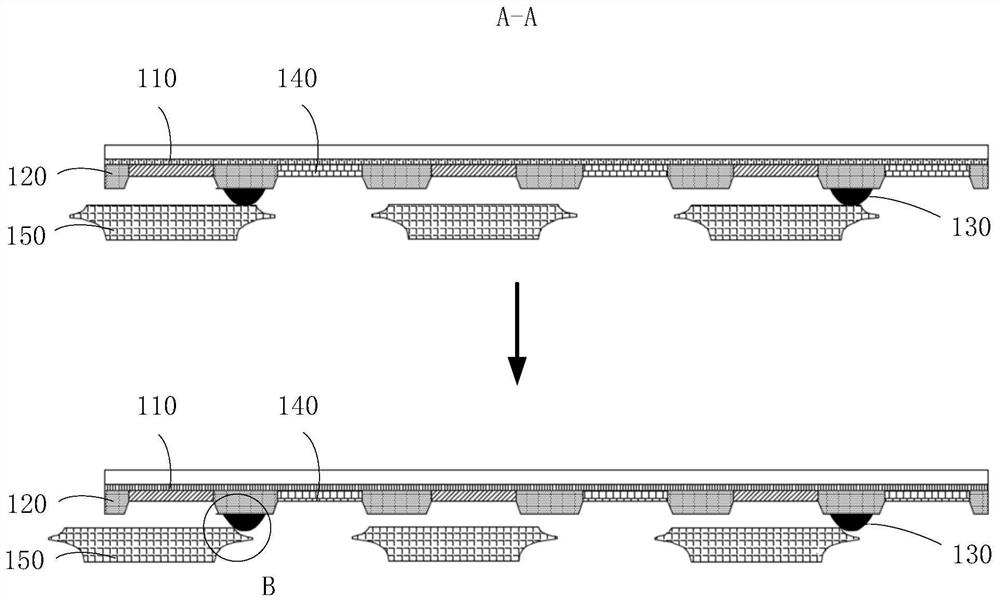
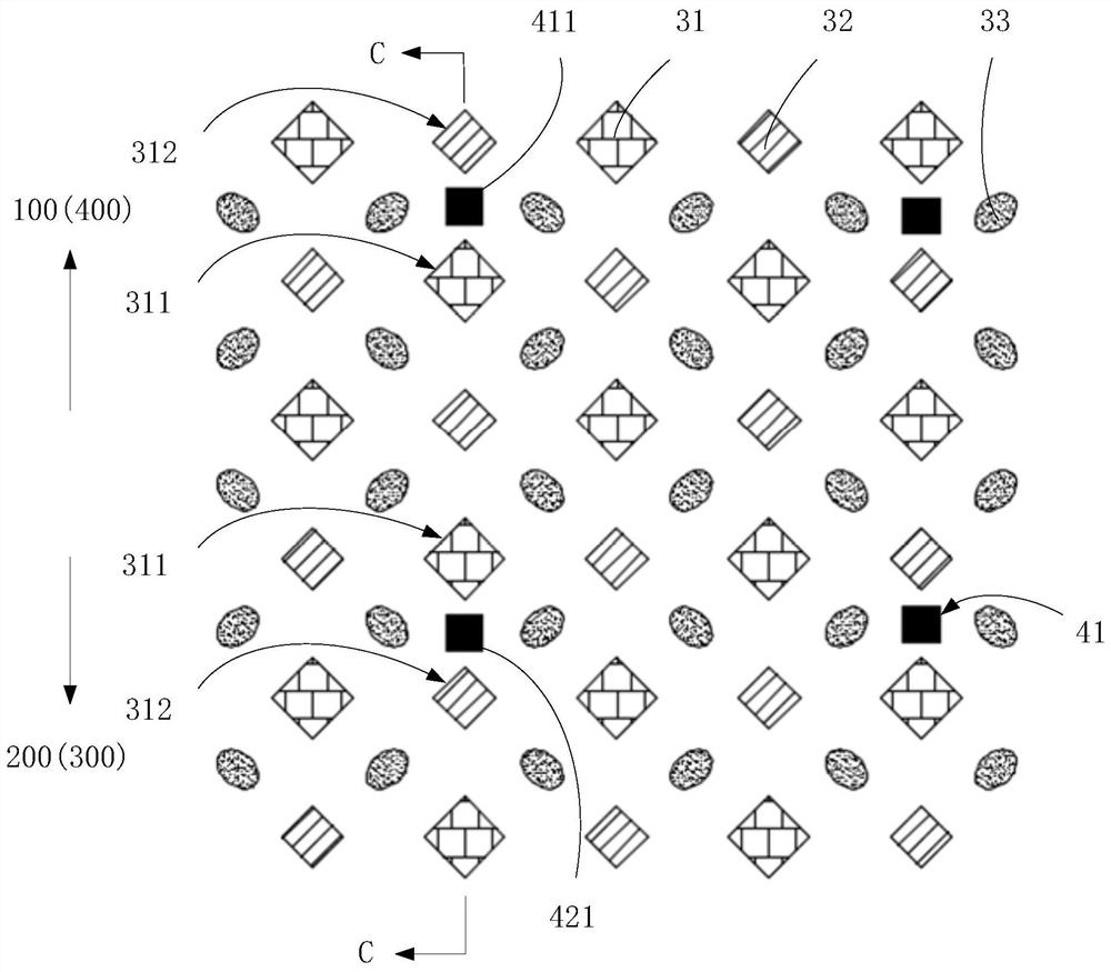
[0041] The following will clearly and completely describe the technical solutions in the embodiments of the application with reference to the drawings in the embodiments of the application. Apparently, the described embodiments are only some of the embodiments of the application, not all of them. Based on the embodiments in this application, all other embodiments obtained by those skilled in the art without making creative efforts belong to the scope of protection of this application. In addition, it should be understood that the specific implementations described here are only used to illustrate and explain the present application, and are not intended to limit the present application. In this application, unless stated to the contrary, the used orientation words such as "up" and "down" usually refer to up and down in the actual use or working state of the device, specifically the direction of the drawing in the drawings ; while "inside" and "outside" refer to the outline of ...


PUM


Abstract

The embodiment of the invention discloses a display panel. According to the display panel, a plurality of first shock insulator columns are distributed according to a first preset rule, so that the first shock insulator columns are in one-to-one correspondence with adjacent first sub-pixel openings, and the first sub-pixel openings are formed in at least two directions around the adjacent first shock insulator columns; in other words, the first shock insulator columns are arranged in different directions of the first sub-pixel openings, and the positions of the pixel openings correspond to the positions of the openings of the mask plate, so that when the mask plate is staggered, all the first shock insulator columns are prevented from sliding into the opening positions of the mask plate at the same time, and when one shock insulator column slides into the opening position of the mask plate, the other shock insulator column can play a supporting role, so that the shock insulator column sliding into the opening position of the mask plate is prevented from being scratched, the probability of generating fine particles is further reduced, and packaging failure or abnormal display of the display panel is avoided.

Description

technical field [0001] The present application relates to the display field, in particular to a display panel. Background technique [0002] Organic light-emitting diode display (OLED, Organic Light-Emitting Diode) is widely used because of its advantages such as high luminous efficiency and fast response speed, such as Figure 1 to Figure 2 As shown, manufacturing an OLED display panel mainly includes the steps of sequentially forming an array substrate 110, a pixel definition film layer 120, a spacer support column 130, a light-emitting function film layer 140, and an encapsulation film layer. In the process of forming the light-emitting functional film layer 140, it is necessary to attach a mask structure such as a fine metal mask 150 (FMM, Fine Metal Mask) to the spacer support column 130, so as to realize the alignment of the spacer support column 130 with the fine metal mask. The support of the mask plate 150 is then formed by vapor deposition of luminescent functional...

Claims


Application Information

Patent Timeline
Patent Type & Authority Applications(China)
IPC IPC(8): H01L27/32H01L51/52
CPCH10K59/12H10K50/8428
Inventor 曹祖强
Owner WUHAN CHINA STAR OPTOELECTRONICS SEMICON DISPLAY TECH CO LTD
Why Eureka
Try Eureka