Method and system for sorting chips into BIN

A chip and sorting technology, applied in image analysis, still image data clustering/classification, image data processing, etc., can solve the problems of low efficiency, long time consumption of LED chips, low precision, etc., to improve scanning resolution, improve Efficiency and the effect of improving sorting accuracy

Pending Publication Date: 2021-10-01
HCP TECH CO LTD
View PDF5 Cites 1 Cited by
  • Summary
  • Abstract
  • Description
  • Claims
  • Application Information

AI Technical Summary

Problems solved by technology

Using this method to sort into the Bin, the test sorter must wait for the Bin file to be completely created before it can start the analysis of the LED chip, which not only makes the entire analysis of the LED chip (from file building to sorting) time-consuming Long, low efficiency, and low precision

Method used


Image

  • Method and system for sorting chips into BIN
  • Method and system for sorting chips into BIN
  • Method and system for sorting chips into BIN

Examples


Embodiment Construction

[0034] In order to describe the technical content, structural features, achieved goals and effects of the present invention in detail, the following will be described in detail in conjunction with the embodiments and accompanying drawings.

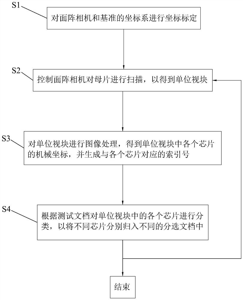
[0035] This embodiment discloses a method for chip sorting into BIN, which is used to establish a sorting document for a number of chips on the mother chip that has passed the test process and has generated test documents, especially for LED chip test sorting work, for test sorting The sorting machine provides sorting data, that is, the sorting test machine performs sorting work on each chip on the master chip according to the sorting document. In this embodiment, the master is located on a base platform, and an area array camera for area image scanning is provided, such as figure 1 , the method of sorting into BIN specifically includes:

[0036] S1: Calibrate the coordinate system of the area array camera and the abutment to obtain the s...


PUM


Abstract

The invention discloses a method and a system for sorting chips into a BIN. The method comprises the following steps of calibrating a coordinate system of an area-array camera and a base station for placing a master slice, controlling the area-array camera, and scanning the master slice according to a preset scanning route and a preset movement interval to obtain unit view blocks at all positions on the master slice, acquiring pixel coordinates of each chip in any unit visual block through an image processing technology, then converting the pixel coordinates into mechanical coordinates, and generating index numbers corresponding to each chip in the current unit visual block, classifying the chips in the current unit visual block according to the test document so as to respectively classify the plurality of chips in the current unit visual block into different sorting documents. According to the method for sorting the chips into the BIN, the test sorting machine can sort the chips according to the sorting documents generated in real time without waiting for the completion of establishment of the sorting documents of the whole master slice, so that the efficiency and the precision of the chip sorting work are effectively improved.

Description

technical field [0001] The invention relates to the technical field of chip sorting, in particular to a method and system for sorting chips into a BIN. Background technique [0002] After the chip packaging is completed, it is generally selected and stored according to different parameters to meet the needs of use. For example, packaged LED chips can be tested and sorted according to wavelength, luminous intensity, luminous angle, and operating voltage. The standard packs the LEDs in different Bin boxes. Due to people's higher and higher requirements for LEDs, the early sorting machine was 32Bin, and later increased to 64Bin. [0003] The traditional test and sorting technology for LED chips generally adopts the method of building a Bin file after scanning the whole. The specific process is as follows: after generating the test file, the sorting machine scans the master chip to generate a scanned file, and finally scans the scanned file and test The documents are combined...

Claims


Application Information

Patent Timeline
Patent Type & Authority Applications(China)
IPC IPC(8): G06T7/80G06T7/00G06F16/51G06F16/55
CPCG06T7/80G06T7/0004G06F16/51G06F16/55G06T2207/10052G06T2207/30148G06T2207/30244
Inventor 林子钦
Owner HCP TECH CO LTD
Why Eureka
Try Eureka