Mode converter and manufacturing method for mode converter
A mode converter and wave mode technology, which is applied in the directions of waveguide-type devices, waveguides, electrical components, etc., can solve the problems of increased man-hours in the manufacturing method of mode converters.
- Summary
- Abstract
- Description
- Claims
- Application Information
AI Technical Summary
Problems solved by technology
Method used
Image
Examples
no. 1 approach 〕
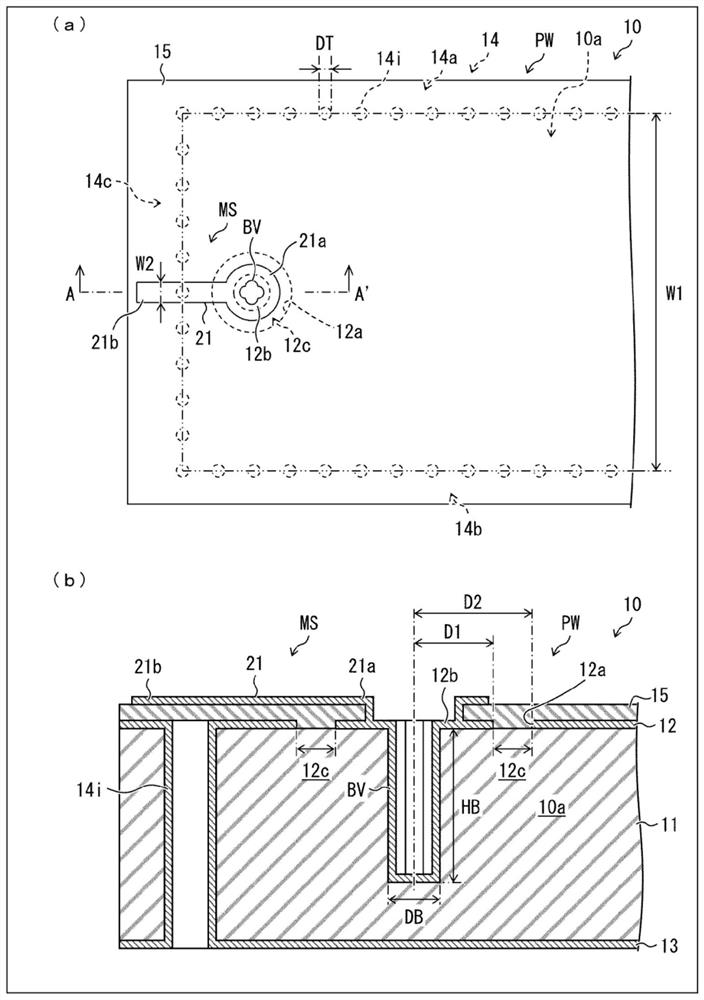
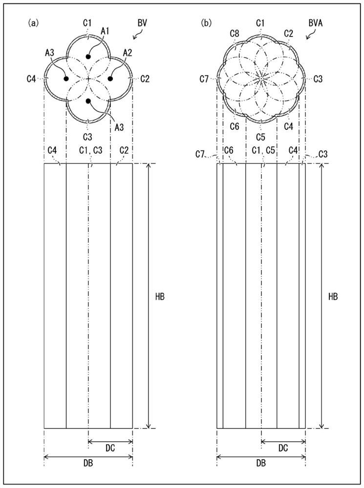
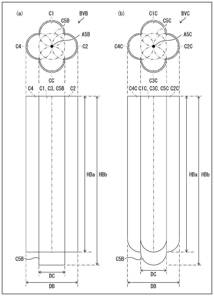
[0026] Hereinafter, reference Figure 1 ~ 3 The mode converter according to the first embodiment of the present invention will be described. figure 1 (A) is a top view of the mode converter 10 according to the present embodiment. figure 1 (B) is an enlarged cross-sectional viewmap in the vicinity of the blind hole BV provided by the mode converter 10. figure 2 (A) is a top view and a side view of a blind hole BV. figure 2 (B) is a top view and a side view of a blind hole BVA as a first modification of the blind hole BV. image 3 (A) is a top view and a side view of a blind hole BVB as a second modification of the blind hole BV. image 3 (B) is a top view and a side view of a blind hole BVC as a third modification of the blind hole BV.
[0027]
[0028] like figure 1 (A) and figure 1 (B), the mode converter 10 includes a post wall waveguide PW, a microstrip line MS, and a blind hole BV.
[0029] (Column wall waveguide PW)
[0030] like figure 1 (B), the column wall waveguide PW inclu...
no. 2 approach 〕
[0065] Refer Figure 4 The manufacturing method M10 of the second embodiment of the present invention is described, and the method M10 of the above-described mode converter 10 will be described. In the present embodiment, the manufacturing method M10 will be described as an example of the blind hole BV, but according to each blind hole BVA, BVB, BVC can also be manufactured in the same manner. Further, in order to facilitate explanation, the description related to the blind hole BV is not repeated.
[0066] like Figure 4 As shown, the manufacturing method M10 includes: a step S11 forming a plurality of through holes and non-through holes; and forming the conductor layers 12, 13, through holes 14i, and blind holes S12. Each of the steps S11 and the step S12 is an example of the first step and the second step described in the scope of the claim. Further, in the present embodiment, in the step S12, the case where the conductor layers 12, 13, through holes 14i, and blind hole BV are fo...
no. 1 example
[0083] Will have figure 2 The embodiment group of the mode converter 10 of the blind hole BV shown in (a) is set to the first embodiment of the present invention. Figure 5 It is a graph showing the reflection characteristics of the mode converter 10 of the first embodiment.
[0084] In the first embodiment, the thickness of the substrate 11 is also set to 700 μm, and the width W1 of the column wall waveguide PW is set to 4 mm, and the width W2 of the microstrip wire 21 is set to 200 μm. On this basis, the height Hb of the cylinder C1 to C4 of the fitted blind hole BV is 550 μm or more and 650 μm or less, 12.5 μm (reference Figure 5 ).
[0085] Refer Figure 5 It can be seen that the mode converter 10 of the first embodiment is shown in the case where the height Hb is 587.5 μm or more and 637.5 μm or less, and in the case of HB = 625 μm, the best reflection is shown within the operating frequency band. characteristic. In particular, it is understood that the mode converter 10 as an ...
PUM
 Abstract
Description
Claims
Application Information
 - R&D
- Intellectual Property
- Life Sciences
- Materials
- Tech Scout
- Unparalleled Data Quality
- Higher Quality Content
- 60% Fewer Hallucinations
Browse by: Latest US Patents, China's latest patents, Technical Efficacy Thesaurus, Application Domain, Technology Topic, Popular Technical Reports.
© 2025 PatSnap. All rights reserved.Legal|Privacy policy|Modern Slavery Act Transparency Statement|Sitemap|About US| Contact US: help@patsnap.com


