Organic light-emitting device

An electroluminescent device and a luminescent technology, applied in the direction of electric solid-state devices, electrical components, semiconductor devices, etc., can solve problems such as increasing the use of evaporation sources, increasing device voltage, and limiting the commercialization of OLEDs

Pending Publication Date: 2021-09-10
合肥鼎材科技有限公司
View PDF0 Cites 0 Cited by
  • Summary
  • Abstract
  • Description
  • Claims
  • Application Information

AI Technical Summary

Problems solved by technology

[0003] In order to improve the device efficiency, OLED devices are often prepared by the double-body method of the light-emitting layer. Although the luminous efficiency is improved to a certain extent, at the same time, the use of evaporation sources is increased, and the preparation is slightly difficult, which limits the commercial development of OLEDs.
[0004] In OLED devices, it is known that hole transport is generally faster than electrons, and the recombination region of the light-emitting layer will be biased towards the direction of the ET layer, resulting in adverse consequences such as reduced device efficiency; although the increase in the thickness of the hole transport layer slows down the flow of holes to the cathode transmission, but it increases the voltage of the device. At the same time, the energy level barrier between different material layers leads to a large accumulation of positive load carriers at their respective interfaces, which reduces the efficiency of the device.
[0005] In recent years, people in the industry have made continuous attempts and explorations to improve device efficiency and stability. Most of them seek new materials to improve device performance, and a large number of novel materials have been developed for electron transmission. Although they have certain effects on device performance However, there are still a large number of accumulations of carriers at the interface, and there are also problems of high device voltage and short life.

Method used


Image

  • Organic light-emitting device
  • Organic light-emitting device
  • Organic light-emitting device

Examples


preparation example Construction

[0086] Preparation of Compound 1-1

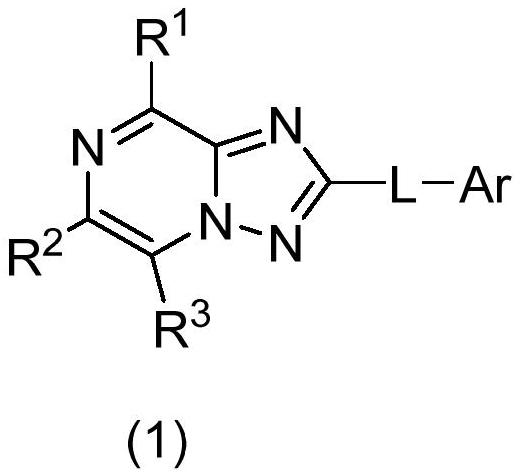
[0087] Single-neck flask was added 2-amino-5-bromo-pyrazine (17.3g, 100mmol), phenanthrene boronic acid (22.2g, 1000mmol), potassium carbonate (41.4g, 300mmol), [1,1'- bis (diphenylphosphino yl) ferrocene] dichloropalladium (0.73g, 1mmol), a solvent of tetrahydrofuran was added 300mL, water 60mL, reaction was refluxed overnight under nitrogen 80 ℃. Solid precipitated out during the reaction. TLC indicated completion of the reaction starting material, the reaction was stopped was cooled to room temperature, the precipitated solid was filtered and rinsed with water and ethanol, respectively, and dried. To give the title compound 1-1 (24.4g, yield 90%).

[0088] Preparation of Compound 1-2

[0089] Intermediate compound 1-1 (22.6g, 83.33mmol) was added with DCM (100mL) in the flask was cooled to 0 deg.] C, was slowly added dropwise ethoxycarbonyl isothiocyanate (10.92g, 83.33mmol), the The reaction solution was elevated to room temperature and sti...

Embodiment 1-1

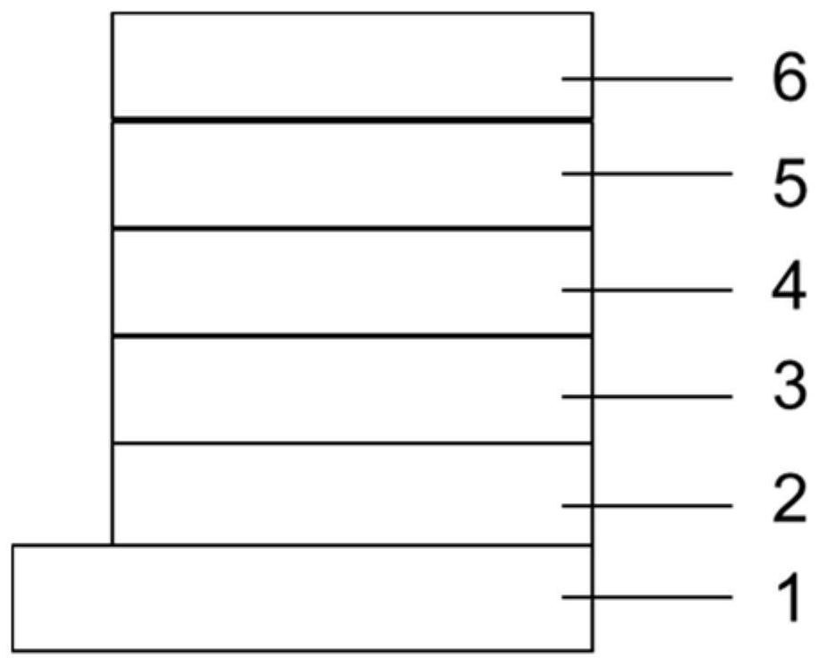
[0136] The glass plate coated with a transparent ITO conductive layer was sonicated in a commercial detergent, rinsed in deionized water, in acetone: ethanol solvent mixture ultrasonic degreasing, baked in a clean environment to completely remove moisture, UV light and ozone cleaning, and low-energy beam strikes the surface of the cation;

[0137] The above-described glass substrate with an anode placed in a vacuum chamber evacuated to 1 × 10 -5 ~ 9 × 10 -3 PA, in the anode layer HT1 film vacuum deposition as a hole transport layer of the device, deposition rate is 0.1nm / s, the total film thickness of 80nm is deposited;

[0138] A light emitting layer on the hole transport layer, light emitting layer comprises a vacuum deposition device, and a host material BFH-1 dye BFD-1, using the multi-source method of co-evaporation of the host material rate is 0.1nm / s, the rate of dye 0.005nm / s, the total film thickness was deposited 20nm.

[0139]Secondary electron emitting layer on t...

Embodiment 1-2

[0144] The glass plate coated with a transparent ITO conductive layer was sonicated in a commercial detergent, rinsed in deionized water, in acetone: ethanol solvent mixture ultrasonic degreasing, baked in a clean environment to completely remove moisture, UV light and ozone cleaning, and low-energy beam strikes the surface of the cation;

[0145] The above-described glass substrate with an anode placed in a vacuum chamber evacuated to 1 × 10 -5 ~ 9 × 10 -3 PA, in the anode layer HT1 film vacuum deposition as a hole transport layer of the device, deposition rate is 0.1nm / s, the total film thickness of 80nm is deposited;

[0146] A light emitting layer on the hole transport layer, light emitting layer comprises a vacuum deposition device, and a host material BFH-1 dye BFD-1, using the multi-source method of co-evaporation of the host material rate is 0.1nm / s, the rate of dye 0.005nm / s, the total film thickness was deposited 20nm.

[0147] Secondary electron emitting layer on ...


PUM

PropertyMeasurementUnit
thicknessaaaaaaaaaa
thicknessaaaaaaaaaa
thicknessaaaaaaaaaa

Abstract

The invention relates to the field of organic electroluminescence, in particular to an organic light-emitting device adopting a novel functional material scheme. The organic light-emitting device comprises an anode, a cathode and one or more organic layers located between the anode and the cathode, the organic layers comprise a light-emitting layer and an electron auxiliary layer, and the electron auxiliary layer is located between the light-emitting layer and the cathode. The electron auxiliary layer comprises a compound as shown in the following formula (1). The organic light-emitting device disclosed by the invention has low starting voltage, high luminous efficiency and longer service life, and can meet the requirements of current panel manufacturing enterprises on high-performance materials.

Description

Technical field [0001] The present invention relates to the field of organic electroluminescent light, and more particularly to an organic electroluminescent device employing a new type of functional material. Background technique [0002] An organic electroluminescence (OLED: Organic Light EMISSION DIODES) device is a class of devices having a class of sandwich structures including a positive and negative electrode film layer and an organic functional material layer clamping between the electrode film layer. The electrode of the OLED device is applied, and the positive charge is injected from the positive electrode, the negative charge is injected from the negative electrode, and the positive and negative charge under the electric field is migrated in the organic layer. Since the OLED devices have the advantages of high brightness, fast response, high viewing angle, simple process, flexibility, etc., are highly received in the new display technology and new lighting technology. ...

Claims


Application Information

Patent Timeline
Patent Type & Authority Applications(China)
IPC IPC(8): H01L51/54H01L51/50
CPCH10K85/622H10K85/615H10K85/654H10K85/6576H10K85/6574H10K85/6572
Inventor 吴俊宇孙恩涛
Owner 合肥鼎材科技有限公司
Why Eureka
Try Eureka