Pixel multiplexing display method and device, storage medium and terminal equipment

A technology of pixel multiplexing and display method, applied in static indicators, instruments, etc., can solve the problems of increasing product cost, increasing the difficulty of chip and mass transfer, etc., to reduce product cost and solve the existing technology of high-resolution display The complex effects of Micro-LED component fabrication and mass transfer process

Active Publication Date: 2021-09-07
KONKA GROUP
View PDF9 Cites 3 Cited by
  • Summary
  • Abstract
  • Description
  • Claims
  • Application Information

AI Technical Summary

Problems solved by technology

Then, if you want to increase the pixel density PPI, you need to reduce the pixel pitch value, increase the number of LED chips and reduce the size of LEDs, which will inevitably increase the difficulty of chips and mass transfer, thereby increasing product costs

Method used


Image

  • Pixel multiplexing display method and device, storage medium and terminal equipment
  • Pixel multiplexing display method and device, storage medium and terminal equipment
  • Pixel multiplexing display method and device, storage medium and terminal equipment

Examples


Embodiment Construction

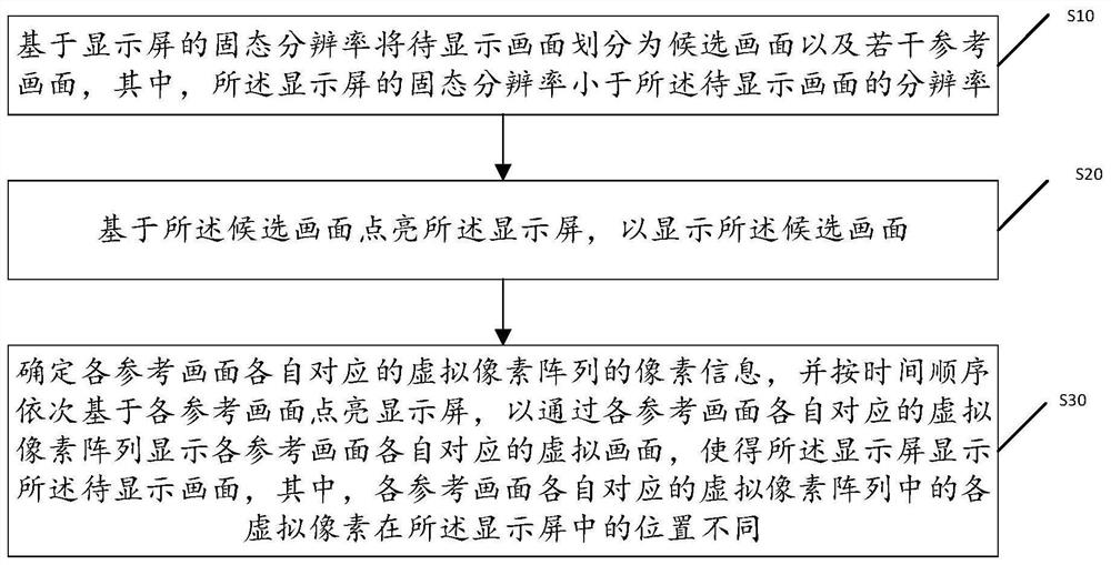
[0037] The present application provides a pixel multiplexing display method, device, storage medium and terminal equipment. In order to make the purpose, technical solution and effect of the present application clearer and clearer, the present application will be further described in detail below with reference to the accompanying drawings and examples. It should be understood that the specific embodiments described here are only used to explain the present application, not to limit the present application.

[0038] Those skilled in the art will understand that unless otherwise stated, the singular forms "a", "an", "said" and "the" used herein may also include plural forms. It should be further understood that the word "comprising" used in the specification of the present application refers to the presence of the features, integers, steps, operations, elements and / or components, but does not exclude the presence or addition of one or more other features, Integers, steps, opera...


PUM


Abstract

The invention discloses a pixel multiplexing display method and device, a storage medium and terminal equipment. The method comprises the steps: dividing a to-be-displayed picture into candidate pictures and a plurality of reference pictures based on the solid-state resolution of a display screen; lightening a display screen based on the candidate picture to display the candidate picture; determining pixel information of the virtual pixel array of each reference picture, and sequentially lightening the display screen based on each reference picture according to a time sequence so as to display a virtual picture corresponding to each reference picture through the virtual pixel array of each reference picture, so that the display screen displays a picture to be displayed. The virtual pixel array is formed on the display screen, and the virtual picture corresponding to the reference picture is displayed through the virtual pixel array, so that the display screen displays the to-be-displayed picture with the resolution higher than the resolution of the display screen, and the high-resolution display picture can be displayed on the basis of the solid resolution, so the problem that the manufacturing and mass transfer process of high-resolution display products is complex is solved, and the product cost is reduced.

Description

technical field [0001] The present application relates to the field of display technology, and in particular to a pixel multiplexing display method, device, storage medium and terminal equipment. Background technique [0002] Micro LED is a new generation of display technology, which has higher brightness and better luminous efficiency than the existing OLED technology, but lower power consumption. Micro LED technology, that is, LED miniaturization and matrix technology, refers to a high-density micro-sized LED array integrated on a chip. For example, each pixel of an LED display can be addressed and individually driven to light up, which can be regarded as A miniature version of the outdoor LED display, reducing the pixel distance from millimeters to microns. [0003] At present, products using Micro-LED generally use RGB three-color chips as a pixel, or use blue light plus QDCC to complete color conversion, and both need to use three LED chips as a pixel. Then, if you wa...

Claims


Application Information

Patent Timeline
Patent Type & Authority Applications(China)
IPC IPC(8): G09G3/32
CPCG09G3/32
Inventor 杨梅慧林伟瀚
Owner KONKA GROUP
Why Eureka
Try Eureka