Array substrate, display panel and display device

A technology of array substrates and driving circuits, which is applied in the field of display panels, display devices, and array substrates, and can solve the problems of high power consumption of μLED products

Pending Publication Date: 2021-08-31
BOE TECH GRP CO LTD
View PDF13 Cites 2 Cited by
  • Summary
  • Abstract
  • Description
  • Claims
  • Application Information

AI Technical Summary

Problems solved by technology

[0004] In view of the shortcomings of the existing methods, the present application proposes an array substrate, a display panel and a display device to solve the technical problem of high power consumption of μLED products in the prior art

Method used


Image

  • Array substrate, display panel and display device
  • Array substrate, display panel and display device
  • Array substrate, display panel and display device

Examples


Embodiment Construction

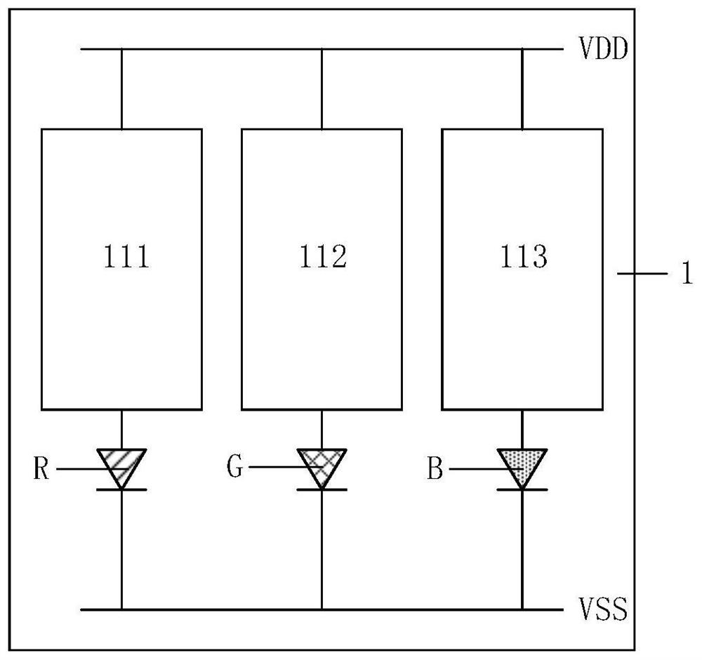
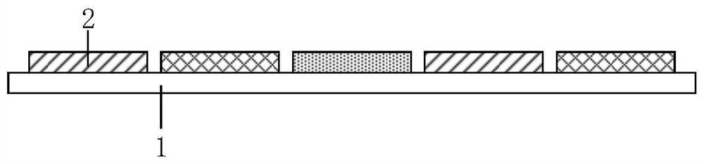
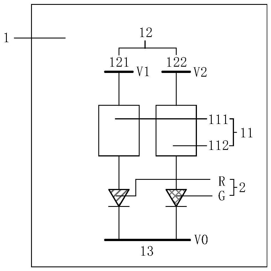
[0044] The present application is described in detail below, and examples of embodiments of the present application are shown in the drawings, wherein the same or similar reference numerals denote the same or similar components or components having the same or similar functions throughout. Also, detailed descriptions of known technologies will be omitted if they are not necessary to illustrate the features of the present application. The embodiments described below by referring to the figures are exemplary only for explaining the present application, and are not construed as limiting the present application.

[0045] Those skilled in the art can understand that, unless otherwise defined, all terms (including technical terms and scientific terms) used herein have the same meanings as commonly understood by those of ordinary skill in the art to which this application belongs. It should also be understood that terms, such as those defined in commonly used dictionaries, should be ...


PUM


Abstract

The embodiment of the invention provides an array substrate, a display panel and a display device. The array substrate bears a plurality of light-emitting units with different colors and comprises a plurality of pixel driving circuits and a plurality of light-emitting units, wherein the pixel driving circuits comprise a first driving circuit and a second driving circuit which are used for driving the light-emitting units with the different colors; the first power supply input end comprises a first sub-input end electrically connected with the first driving circuit and a second sub-input end electrically connected with the second driving circuit, the first sub-input end inputs a first voltage to the first driving circuit, and the second sub-input end inputs a second voltage different from the first power supply to the second driving circuit. According to the array substrate, the non-light-emitting invalid power consumption of the light-emitting unit needing small driving current can be reduced, so that the power consumption of the array substrate is reduced.

Description

technical field [0001] The present application relates to the field of display technology, and in particular, the present application relates to an array substrate, a display panel and a display device. Background technique [0002] μLED (Ultra Light Emitting Diode, Extreme Light Emitting Diode) includes Micro LED or submillimeter light emitting diode Mini LED. By integrating μLED with high density on the array substrate, each μLED can be addressed and emit light individually. [0003] The driving current of each light-emitting unit in the μLED display device can reach tens of uA to hundreds of uA, which is on the order of a thousand times the nA-level driving current in OLED (organic light-emitting diode) products, while μLED products have higher power consumption is one of its problems. Contents of the invention [0004] In view of the shortcomings of the existing methods, the present application proposes an array substrate, a display panel and a display device to solve...

Claims


Application Information

Patent Timeline
IPC IPC(8): G09G3/32
CPCG09G3/32H10K59/12H01L25/0753H01L25/167G09G3/3233H10K59/35H10K59/1213H10K59/30H10K59/131H10K59/1216H10K59/1201
Inventor 刘冬妮玄明花郑皓亮赵蛟
Owner BOE TECH GRP CO LTD
Why Eureka
Try Eureka