Resin molded article for sealing optical semiconductor, optical semiconductor sealing material, and optical semiconductor device

An optical semiconductor device and optical semiconductor technology, which are applied in the fields of semiconductor devices, semiconductor/solid-state device manufacturing, semiconductor/solid-state device components, etc., can solve the problem of cracking of small pieces of resin, and achieve the effect of not easy to crack and excellent optical properties.

Pending Publication Date: 2021-08-27
NITTO DENKO CORP
View PDF1 Cites 0 Cited by
  • Summary
  • Abstract
  • Description
  • Claims
  • Application Information

AI Technical Summary

Problems solved by technology

In addition, conventional resin pellets for encapsulating optical semiconductors containing a large amount of fine powder have the problem of being prone to cracks

Method used


Image

  • Resin molded article for sealing optical semiconductor, optical semiconductor sealing material, and optical semiconductor device
  • Resin molded article for sealing optical semiconductor, optical semiconductor sealing material, and optical semiconductor device

Examples


Embodiment 1~4 and comparative example 1~3

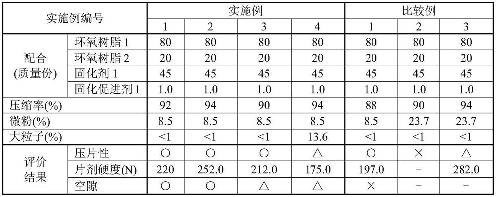
[0069] Heat, melt and mix each raw material in an extruder set at 130°C in the compounding amount shown in Table 1, and then mold the resin discharged from the discharge port of the extruder into a thickness of 2mm to 10mm. Under heat treatment for 60 minutes, an epoxy resin composition was obtained. The resulting epoxy resin composition was granulated by a dry compression granulator, then pulverized with a turbo mill, and then 120 mesh sieves and 10 mesh sieves were used to adjust the particle diameter as shown in Table 1. The micropowder and The proportion of large particles with a particle size of 2000 μm or more. Then, the obtained powder was pelletized into a diameter of 13 mm and a weight of 2.4 g using a rotary tablet press, thereby producing resin pellets for optical semiconductor encapsulating with compression ratios shown in Table 1.

[0070] Using the obtained pellets, tabletability, tablet hardness and voids were evaluated by the following methods. The results ar...

Embodiment 5~8 and comparative example 4~6

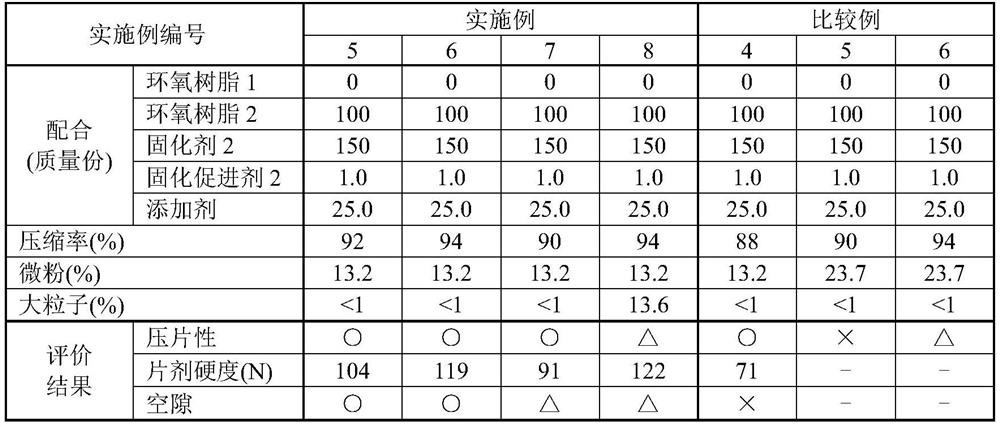
[0085] Except having used each raw material in the compounding quantity shown in Table 2, it carried out similarly to Examples 1-4 and Comparative Examples 1-3, and produced the resin pellet for optical semiconductor encapsulation. Using the obtained pellets, tabletability, tablet hardness and voids were evaluated by the methods described above. The results are shown in Table 2.

[0086] Table 1

[0087]

[0088] Table 2

[0089]


PUM

PropertyMeasurementUnit
Particle sizeaaaaaaaaaa

Abstract

The invention relates to a resin molded article for sealing an optical semiconductor, an optical semiconductor sealing material, and an optical semiconductor device. Provided are: a resin molded article for sealing an optical semiconductor, which is not susceptible to cracks and is not susceptible to voids during molding; an optical semiconductor sealing material obtained using the resin molded article for sealing an optical semiconductor; and an optical semiconductor device. The resin molded article for sealing an optical semiconductor is used in an optical semiconductor sealing material in which the thickness of the thinnest portion is 300 [mu]m or less, and which has a compression ratio of 90% or more and a proportion of particles having a particle diameter of 125 [mu]m or less in the resin molded article for sealing an optical semiconductor of 15% or less.

Description

technical field [0001] The present invention relates to a resin molded article for optical semiconductor encapsulation, an optical semiconductor encapsulation material, and an optical semiconductor device. Background technique [0002] The optical semiconductor element is encapsulated by a ceramic package or a plastic package to form a device. Here, since ceramic packages are relatively expensive in terms of constituent materials and poor in mass production, the use of plastic packages has become the mainstream. Among them, from the viewpoints of workability, mass production, and reliability, the technique of pre-tabletting an epoxy resin composition into a tablet and transferring the resulting molded product has become mainstream. . [0003] By the way, in the epoxy resin composition for optical semiconductor encapsulation used in plastic encapsulation, the components of epoxy resin, curing agent, and curing accelerator are relatively difficult to disperse, and it is diff...

Claims


Application Information

Patent Timeline
IPC IPC(8): C08L63/00H01L23/29
CPCC08L63/00H01L23/293H01L23/295H01L23/296C08L2205/025C08L2203/206C09K3/10H01L21/56H01L33/56H01L31/0203C09K2003/1059
Inventor 藤井宏中山根实松尾晓大田真也姫野直子
Owner NITTO DENKO CORP
Why Eureka
Try Eureka