A voltage self-following anti-backflow circuit
An anti-backfeed and voltage technology, which is applied in the direction of adjusting electrical variables, instruments, control/regulation systems, etc., can solve the problem that the circuit cannot work, the constant current charging anti-backfeed and no pressure loss function cannot be realized, and continuous changes are not allowed, etc. problem, to achieve the effect of preventing backfilling
- Summary
- Abstract
- Description
- Claims
- Application Information
AI Technical Summary
Problems solved by technology
Method used
Image

Examples
Embodiment approach 1
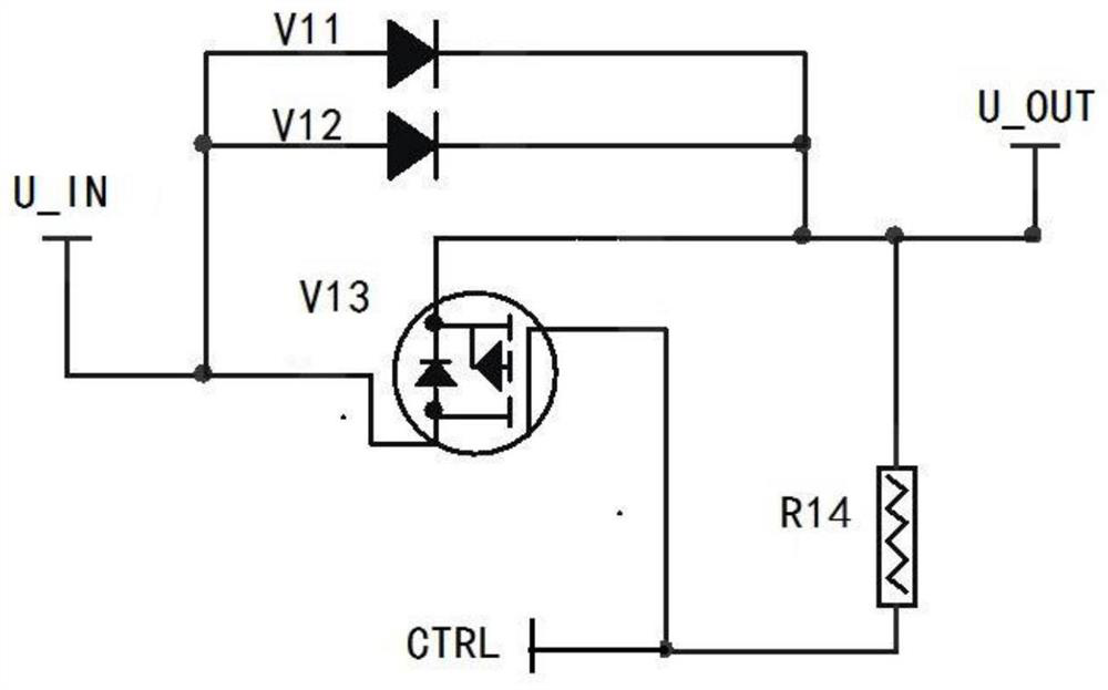
[0028] figure 1 It is a circuit diagram of the first embodiment. like figure 1 As shown, the voltage self-following anti-backflow circuit includes a diode V11, a diode V12, a PMOS transistor V13, and a resistor R14; the voltage input terminal U_IN of the voltage self-following anti-backflow circuit is connected to the diodes V11 and V12. The anodes and all The drain of the PMOS transistor V13, the voltage output terminal U_OUT of the self-following anti-backflow circuit is connected to the cathodes of the diodes V11 and V12 and the source of the PMOS transistor V13, and the gate of the PMOS transistor V13 Connect to the external control signal input terminal CTRL, the external control signal input terminal CTRL can output high and low levels to control the opening and closing of the PMOS transistor V13; one end of the resistor R14 is connected to the source of the PMOS transistor V13, and the other end is connected to the PMOS transistor. The gate of V13. As a more optimal ...
Embodiment approach 2
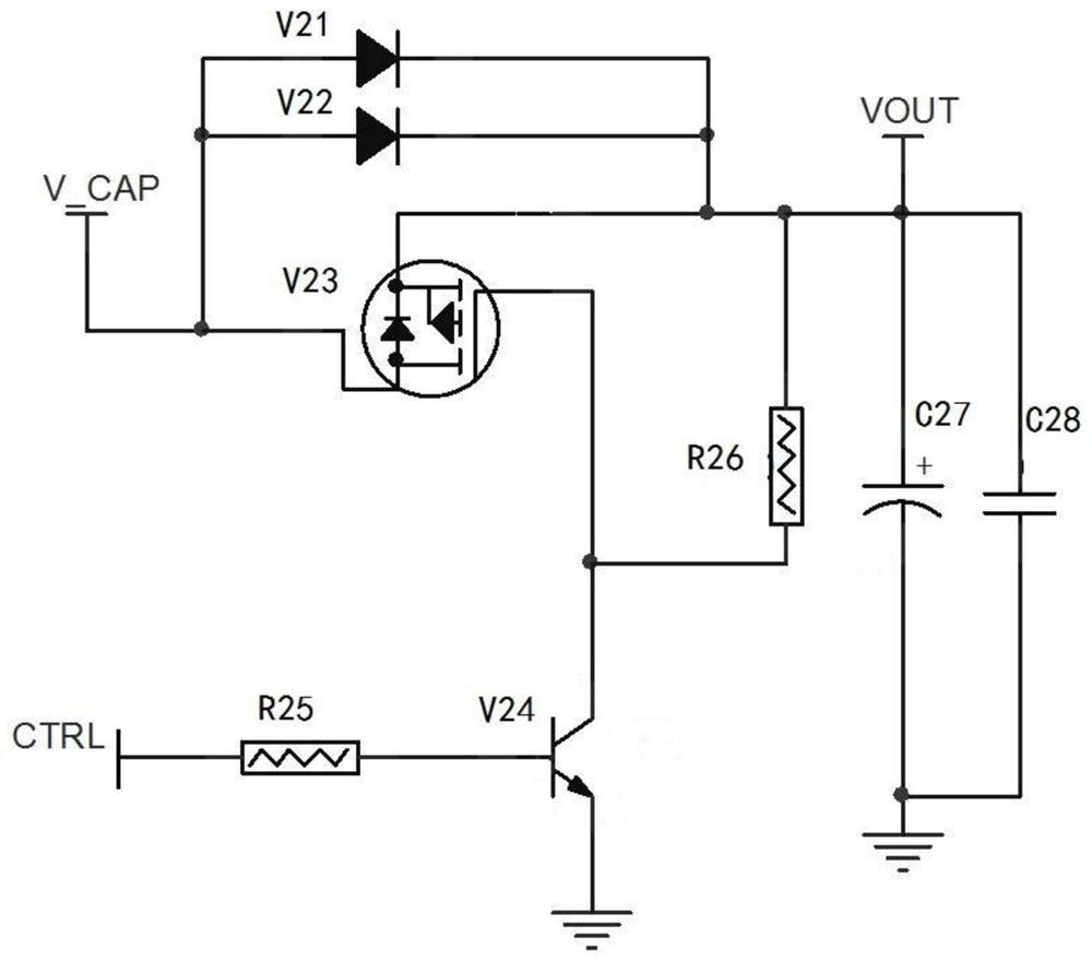
[0033] figure 2 It is a circuit diagram of Embodiment 2 of the present invention. like figure 2 As shown, the voltage self-following anti-backflow circuit includes a diode V21, a diode V22, a PMOS tube V23, a transistor V24, a resistor R25, a resistor R26, a capacitor C27, and a capacitor C28; the voltage self-following anti-backflow circuit The voltage input terminal V_CAP Connect the anodes of the diodes V21 and V22 and the drain of the PMOS transistor V23, and the voltage output terminal VOUT of the self-following anti-backflow circuit is connected to the cathodes of the diodes V21 and V22 and the PMOS transistor V23 the source of the PMOS transistor V23, the gate of the PMOS transistor V23 is connected to the collector of the transistor V24, one end of the resistor R26 is connected to the source of the PMOS transistor V23, and the other end is connected to the gate of the PMOS transistor V23, the The emitter of the transistor V24 is grounded, the base of the transistor...
Embodiment approach 3
[0036] Figure 4 It is a circuit diagram of Embodiment 3 of the present invention. like Figure 4 As shown, the voltage self-following anti-backflow circuit includes a diode V31, a diode V32, a PMOS tube V33, a MOS tube V34, a resistor R35, a resistor R36, a capacitor C37, and a capacitor C38; the voltage self-following anti-backflow circuit voltage input terminal V_CAP is connected to the anodes of the diodes V31 and V32 and the drain of the PMOS transistor V33, and the voltage output terminal VOUT of the self-following anti-backflow circuit is connected to the cathodes of the diodes V31 and V32 and the PMOS transistor The source of V33, the gate of the PMOS transistor V33 is connected to the drain of the MOS transistor V34, one end of the resistor R36 is connected to the source of the PMOS transistor V33, and the other end is connected to the gate of the PMOS transistor V33, The source of the MOS transistor V34 is grounded, the gate of the MOS transistor V34 is connected t...
PUM
 Abstract
Description
Claims
Application Information
 - R&D
- Intellectual Property
- Life Sciences
- Materials
- Tech Scout
- Unparalleled Data Quality
- Higher Quality Content
- 60% Fewer Hallucinations
Browse by: Latest US Patents, China's latest patents, Technical Efficacy Thesaurus, Application Domain, Technology Topic, Popular Technical Reports.
© 2025 PatSnap. All rights reserved.Legal|Privacy policy|Modern Slavery Act Transparency Statement|Sitemap|About US| Contact US: help@patsnap.com