Method for analyzing tin layer thickness of CP leading-out wire for electrolytic capacitor
An electrolytic capacitor and analysis method technology, which is applied in the field of analyzing the thickness of the tin layer of the CP lead-out wire for electrolytic capacitors, can solve the problem that the thickness of the tin layer cannot be measured comprehensively and intuitively, and achieves the effect of easy operation.
- Summary
- Abstract
- Description
- Claims
- Application Information
AI Technical Summary
Problems solved by technology
Method used
Image
Examples
Embodiment 1
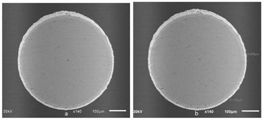
[0037]A method for analyzing the tin layer thickness of a CP lead-out wire for an electrolytic capacitor, comprising the steps of:
[0038] S1. Sampling and inlaying: Fix the lead-out wire of the electrolytic capacitor CP vertically on the upper mold, and use the matching lower mold, and then use acrylic resin for cold embedding and curing;
[0039] S2. Polish the electrolytic capacitor fixed vertically in step S1 with the surface to be tested of the CP lead-out line, and then polish it with 400#, 2000#, and 5000# SiC water sandpaper for 15 minutes, use water as a cleaning agent, and then use The polishing liquid is polished for 15 to 25 minutes, and the particle size of the polishing liquid is 80nm; then the scanning electron microscope is used for analysis, and finally the software Image Pro Plus is used for measurement and analysis. Flow 80uA, Image Pro Plus software Select spatial (select scale). Wherein the fixing method of the sample of this embodiment is as follows: ...
Embodiment 2
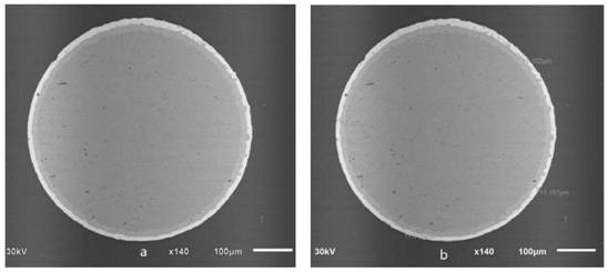
[0041] The analysis method of the tin layer thickness of the CP lead-out wire for the electrolytic capacitor of this embodiment is the same as that of Embodiment 1, the difference is that the working conditions of the scanning electron microscope are replaced by accelerating voltage 30kv, working distance WD12mm, and beam current 90uA.
Embodiment 3
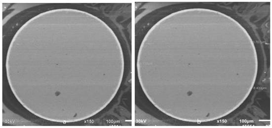
[0043] The analysis method for the thickness of the tin layer of the CP lead wire for electrolytic capacitors in this embodiment is the same as that in Embodiment 1, except that the working conditions of the scanning electron microscope are replaced by accelerating voltage 30kv, working distance WD10mm, and beam current 85uA.
PUM
 Abstract
Description
Claims
Application Information
 - Generate Ideas
- Intellectual Property
- Life Sciences
- Materials
- Tech Scout
- Unparalleled Data Quality
- Higher Quality Content
- 60% Fewer Hallucinations
Browse by: Latest US Patents, China's latest patents, Technical Efficacy Thesaurus, Application Domain, Technology Topic, Popular Technical Reports.
© 2025 PatSnap. All rights reserved.Legal|Privacy policy|Modern Slavery Act Transparency Statement|Sitemap|About US| Contact US: help@patsnap.com


