
Zero-crossing self-calibration circuit, dc/dc converter and power management chip

A self-calibration and zero-crossing technology, applied in the direction of output power conversion devices, instruments, electrical components, etc., can solve the problems of high power loss, large circuit power loss, and limited DC/DC conversion circuit, etc., to avoid excessive discharge Zero, to avoid the effect of indeterminate sensory value

Active Publication Date: 2021-09-07
ZHUHAI JIELI TECH
View PDF0 Cites 0 Cited by
  • Summary
  • Abstract
  • Description
  • Claims
  • Application Information

AI Technical Summary

Problems solved by technology

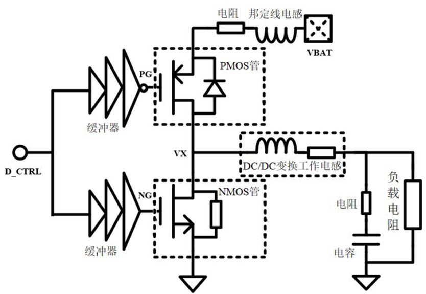
[0002] DC / DC (Direct current-Direct current converter, direct current to direct current) converters are applied to the power management chip side of electronic products. The converter often only integrates the corresponding power tube and control circuit. The inductor on the converter is charged and discharged during the DC / DC step-up voltage conversion process to improve the conversion efficiency and achieve small loss. Large inductors and capacitors are required outside the chip. , often at the uH (microhenry) level, which will result in higher BOM (Bill of Material, bill of materials) costs, and unreasonable use of redundant pins, resulting in limited DC / DC conversion circuits in power supply applications
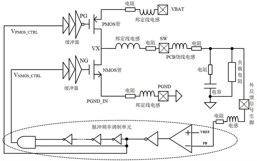
When the inductor works in DCM (Discontinous Conduction Mode, continuous conduction mode) or PFM (Pulse Frequency Modulation, pulse frequency modulation mode), NMOS (N-Metal-Oxide-Semiconductor, N-type metal-oxide-semiconductor) power The conduction time of the tube remains unchanged, and the current crosses zero, which will cause a large power loss
[0003] During the implementation process, the inventors found that there are at least the following problems in the traditional technology: the power loss of the traditional DC / DC conversion circuit is large

Method used


Image

  • Zero-crossing self-calibration circuit, dc/dc converter and power management chip
  • Zero-crossing self-calibration circuit, dc/dc converter and power management chip
  • Zero-crossing self-calibration circuit, dc/dc converter and power management chip

Examples


Embodiment Construction

[0040] In order to understand the present application, the present application will be further described with reference to the related drawings. The embodiment of the present application is given in the drawings. However, the present application can be implemented in many different forms, is not limited to the embodiments described herein. Conversely, the purpose of providing these embodiments is to make the disclosure of the present application more thoroughly.

[0041] All techniques and scientific terms used herein are commonly understood by those skilled in the art, unless otherwise defined. The terms used herein in the specification of the present application are merely intended to describe the embodiments of the specific embodiments, are not intended to limit the present application.

[0042] It will be appreciated that the terms "first", "second", and the like as used herein can be used herein to describe various elements, but these components are not limited by these terms...


PUM


Abstract

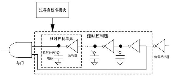
The application relates to a zero-crossing self-calibration circuit, a DC / DC converter and a power management chip. The zero-crossing self-calibration circuit includes: a first power tube, a second power tube, an inductor, a controller, a signal inverter, a feedback signal comparator, a zero-crossing self-calibration module, and a delay control module; wherein, the zero-crossing self-calibration The calibration module is used to obtain and compare the node voltage between the first power tube and the second power tube and the source voltage of the first power tube, obtain the comparison result, and output the adjustment parameter according to the comparison result; the delay control module receives the adjustment parameter And adjust the conduction time of the first power transistor based on the adjustment parameter. This application can realize self-adaptive adjustment of the conduction time of the first power tube, accurately detect the zero-crossing point of the current, avoid the zero-crossing of the inductance discharge, and avoid the indeterminate inductance value of the inductance and the buck-boost conversion power caused by the excessive slope of the inductance The problem of large losses.

Description

Technical field [0001] The present application relates to the field of power management technology, particularly to a self-calibration circuitry through zero, DC / DC converter and power management chip. Background technique [0002] DC / DC (Direct current-Direct current converter, DC to DC) converter is applied to the power management chip end electronics, DC / DC boost converter or buck conversion efficiency gradually widespread attention, common DC / DC converter often only appropriate integrated power transistor and a control circuit, the inductor converter during charge and discharge process DC / DC voltage down conversion, improve the conversion efficiency, while achieving a small loss, it requires a large volume of off-chip inductors and capacitors often uH Tolerance (microhenries) level, will result in a higher BOM (Bill of material, BOM) cost, and the extra pin is not rationally utilized, resulting in DC / DC converter circuit are limited in power applications. When wor...

Claims


Application Information

Patent Timeline
Patent Type & Authority Patents(China)
IPC IPC(8): H02M1/088H02M3/158
CPCH02M1/088H02M3/158
Inventor 杨建新魏荣臣
Owner ZHUHAI JIELI TECH
Learn More