Converter circuit composed of no-loss current buffer circuit
A technology of current buffering and circuit formation, which is applied in the direction of converting DC power input to DC power output, adjusting electrical variables, and converting devices for output power, etc. , The effect of reducing electromagnetic noise emission and avoiding large losses
- Summary
- Abstract
- Description
- Claims
- Application Information
AI Technical Summary
Problems solved by technology
Method used
Image
Examples
Embodiment Construction
[0020] The present invention will be further described below in conjunction with the accompanying drawings and embodiments.
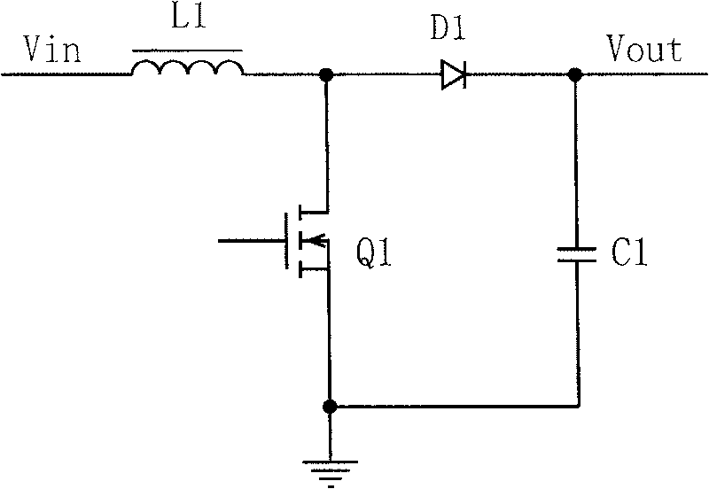
[0021] like figure 1 Shown is the current common Boost converter circuit diagram.
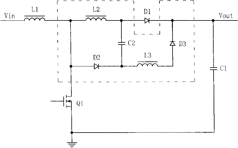
[0022] like figure 2 Shown is the circuit diagram of the first converter composed of a lossless current buffer and a Boost boost converter. it is in figure 1 On the basis of the Boost converter circuit shown above, disconnect the anode of the rectifier D1 from the original circuit; connect the connection point of the buffer inductor L2 and the energy storage capacitor C2 to the anode of the rectifier D1; connect the buffer inductor L2 and the buffer The connection point of the anode of the diode D2 is connected with the drain of the switching tube Q1 and the boost inductor L1, and the cathode of the discharge diode D3 is connected with the cathode of the rectifier D1. The dashed box is a lossless current snubber circuit.
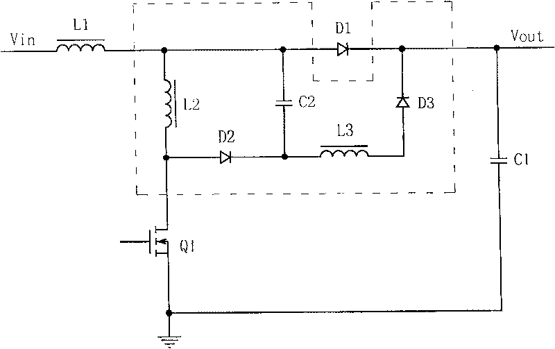
[0023] like image 3 Shown is the circuit...
PUM
 Abstract
Description
Claims
Application Information
 - R&D
- Intellectual Property
- Life Sciences
- Materials
- Tech Scout
- Unparalleled Data Quality
- Higher Quality Content
- 60% Fewer Hallucinations
Browse by: Latest US Patents, China's latest patents, Technical Efficacy Thesaurus, Application Domain, Technology Topic, Popular Technical Reports.
© 2025 PatSnap. All rights reserved.Legal|Privacy policy|Modern Slavery Act Transparency Statement|Sitemap|About US| Contact US: help@patsnap.com


