Miniature light-emitting diode transfer method and display device

A technology of light-emitting diodes and transfer methods, which is applied in the direction of electric solid-state devices, semiconductor devices, transportation and packaging, etc., to achieve the effect of reducing transfer costs and simple and convenient operation

Active Publication Date: 2021-06-18
CHONGQING KONKA PHOTOELECTRIC TECH RES INST CO LTD
View PDF7 Cites 0 Cited by
  • Summary
  • Abstract
  • Description
  • Claims
  • Application Information

AI Technical Summary

Problems solved by technology

[0005] The technical problem to be solved by the present invention is to provide a micro-light-emitting diode transfer method and a display device for the above-mentioned defects of the prior art, aiming at solving the problem that there is no applicable technology with simple operation and low cost in the prior art. The problem of micro-light-emitting diode transfer

Method used


Image

  • Miniature light-emitting diode transfer method and display device
  • Miniature light-emitting diode transfer method and display device
  • Miniature light-emitting diode transfer method and display device

Examples


Embodiment Construction

[0036] In order to make the object, technical solution and advantages of the present invention more clear and definite, the present invention will be further described in detail below with reference to the accompanying drawings and examples. It should be understood that the specific embodiments described here are only used to explain the present invention, not to limit the present invention.

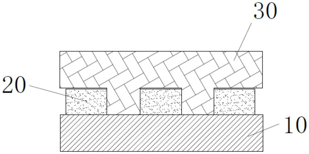
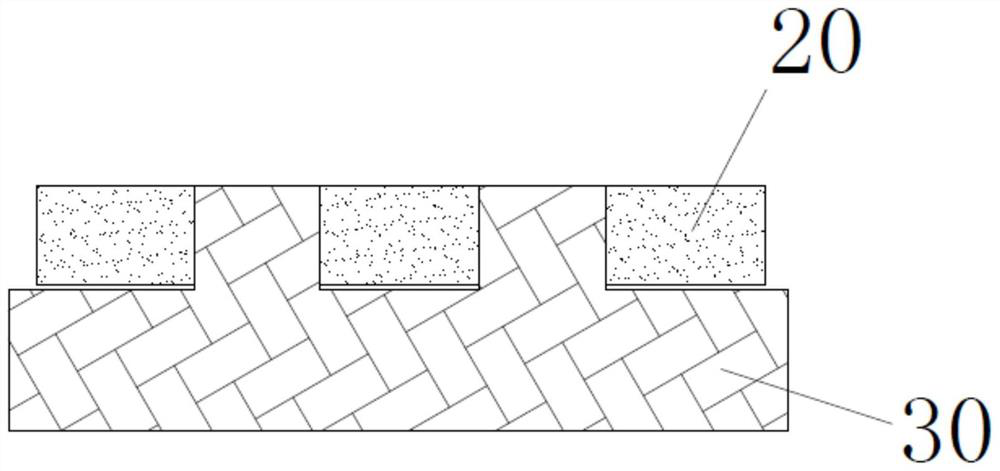
[0037] Since the development of miniature light-emitting diodes, the key technologies of mass transfer include electrostatic adsorption technology, fluid assembly technology, roller imprinting technology, Van der Waals force transfer technology, laser transfer technology, etc., but the above-mentioned technologies are complicated and It is expensive and the technology is relatively immature. The invention provides a mass transfer technology of micro light-emitting diodes with simple operation and low cost.

[0038] See figure 1 , figure 1 It is a flow chart of the method for transferr...


PUM


Abstract

The invention provides a micro light-emitting diode transfer method and a display device, and the method comprises the steps: providing a polymer solution, smearing the polymer solution on a plurality of micro light-emitting diodes growing on a growth substrate, and enabling the polymer solution to be solidified when the polymer solution is heated to a preset temperature; curing the polymer solution on the plurality of micro light-emitting diodes to form a polymer film layer; stripping the growth substrate; providing an ultraviolet film, attaching the ultraviolet film to the growth faces of the micro light-emitting diodes, wherein the growth faces are opposite to the faces where the polymer film layer is located; providing a target substrate, and attaching the side, provided with the polymer thin film layer, of the micro light-emitting diode to the target substrate; and stripping the polymer film layer from the ultraviolet film. According to the invention, the micro light-emitting diodes are transferred from the growth substrate to the target substrate, the operation is simple and convenient, and the cost is low.

Description

technical field [0001] The invention relates to the technical field of semiconductor manufacturing, in particular to a micro light emitting diode transfer method and a display device. Background technique [0002] As a new generation of display technology or final display technology, micro LEDs (Micro LED) are much more compact than traditional liquid crystal display (Liquid Crystal Display, LCD) and organic light-emitting diode (OLED) Light-emitting diodes have the advantages of higher brightness, luminous efficiency, better color reproduction, and lower power consumption, so they are favored by the industry. [0003] The advantages of miniature light-emitting diodes come from smaller pitches. Along with the reduction in size, there are also technical difficulties. Traditional LED packaging mainly adopts vacuum adsorption for transfer, but due to the physical limit of vacuum tubes, they can only When reaching 80 μm, the size of the miniature light-emitting diodes is basica...

Claims


Application Information

Patent Timeline
Patent Type & Authority Applications(China)
IPC IPC(8): H01L33/00H01L21/677H01L25/16
CPCH01L33/005H01L33/0095H01L21/67781H01L25/167
Inventor 刘海平许时渊唐彪
Owner CHONGQING KONKA PHOTOELECTRIC TECH RES INST CO LTD
Why Eureka
Try Eureka