Mini LED panel vacuum correction device
A calibration device and vacuum technology, applied in electrical components, semiconductor/solid-state device manufacturing, circuits, etc., can solve the problems of low precision and low efficiency, and achieve the effect of strong practicability, simple structure, and improved detection accuracy and detection efficiency.
- Summary
- Abstract
- Description
- Claims
- Application Information
AI Technical Summary
Problems solved by technology
Method used
Image
Examples
Embodiment Construction
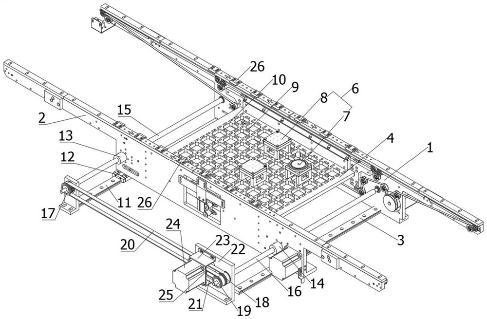
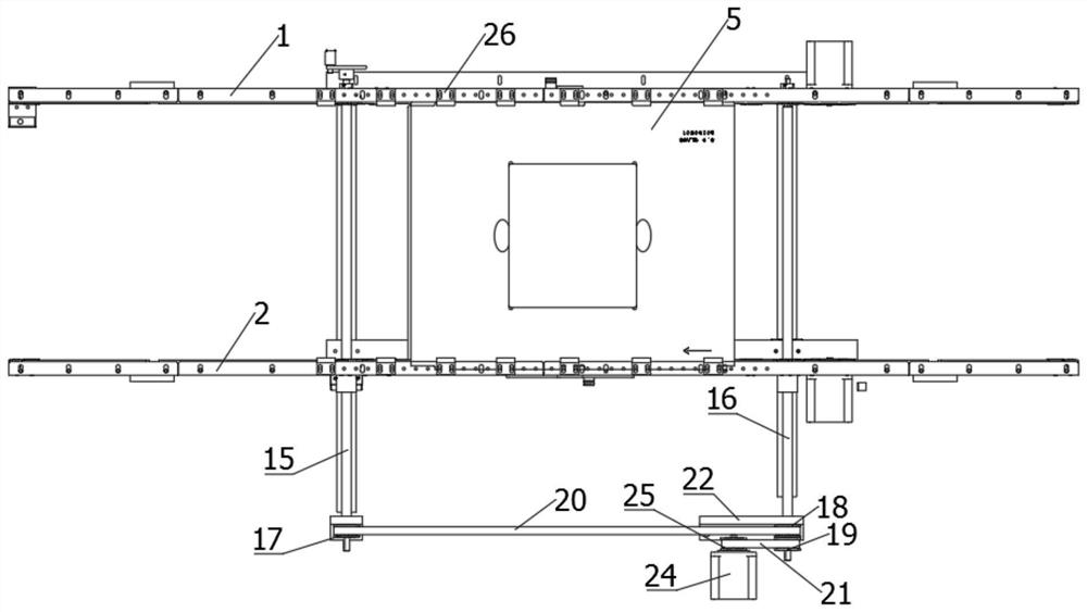
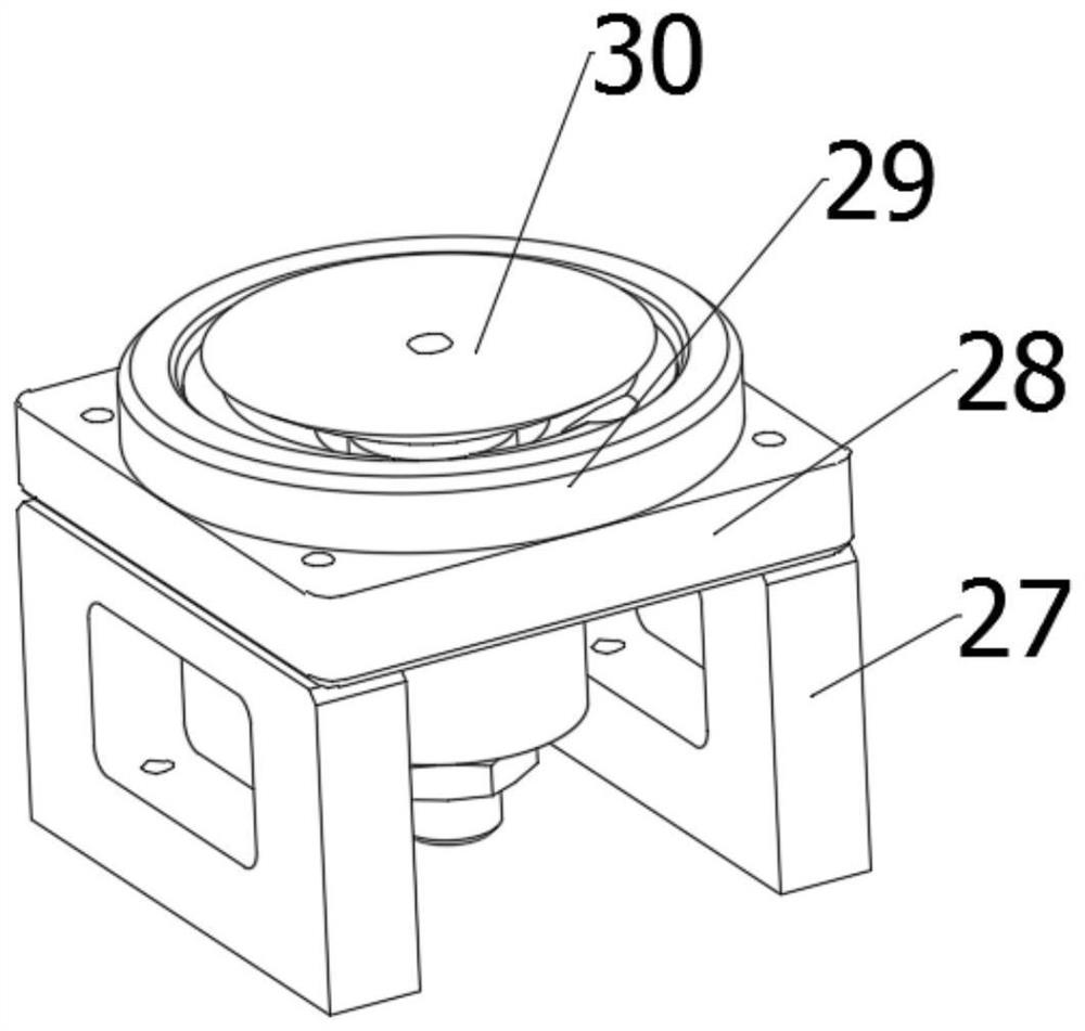
[0022] First of all, the original intention of the design of the present invention is explained. The shape of the plate product is flat, the ratio of width to thickness is large, and the surface area per unit volume is also large. This shape characteristic brings its characteristics in use: (1) The surface area is large, so the ability to contain and cover is strong, ( 2) Can be arbitrarily cut, bent, stamped, welded, and made into various product components. It is made of compound, which can emit visible light when electrons and holes recombine, so it can be used to make light-emitting diodes. At present, with the rapid development of LED manufacturing and packaging industry, the competition among peers is becoming more and more serious, not only in terms of quality To have an advantage, it is necessary to have a unique control method in terms of production cost control. The existing boards commonly used in the market are one piece. The existing LED boards need to be tested du...
PUM
 Abstract
Description
Claims
Application Information
 - R&D
- Intellectual Property
- Life Sciences
- Materials
- Tech Scout
- Unparalleled Data Quality
- Higher Quality Content
- 60% Fewer Hallucinations
Browse by: Latest US Patents, China's latest patents, Technical Efficacy Thesaurus, Application Domain, Technology Topic, Popular Technical Reports.
© 2025 PatSnap. All rights reserved.Legal|Privacy policy|Modern Slavery Act Transparency Statement|Sitemap|About US| Contact US: help@patsnap.com


