Chip capacitor processing equipment

A technology for processing equipment and capacitors, applied in capacitors, capacitor manufacturing, circuits, etc., can solve problems such as large footprint, inability to directly connect stamping machines, incompatibility between stamping machines and pin cutting devices, etc., to improve work efficiency Effect

Active Publication Date: 2021-05-25
FUJICON ELECTRONICS TECH SHAOGUAN
View PDF6 Cites 4 Cited by
  • Summary
  • Abstract
  • Description
  • Claims
  • Application Information

AI Technical Summary

Problems solved by technology

In the production process of capacitors, it is necessary to print relevant information on the outer surface of the capacitor, and cut off the excessively long leads of the capacitor according to the specifications of the capacitor. At present, it is necessary to use a stamping machine and a lead cutting device to complete the above process, occupying an area of The area is large, and due to the differences in the structure and production methods of the two devices, the stamping machine and the pin cutting device are not compatible, and the output end of the stamping machine cannot be directly connected to the feeding end of the pin cutting device.

Method used


Image

  • Chip capacitor processing equipment
  • Chip capacitor processing equipment
  • Chip capacitor processing equipment

Examples


Embodiment Construction

[0028] The present invention will be described in detail below in conjunction with the accompanying drawings and embodiments.

[0029] It is worth noting that the orientation words such as "up" and "down" involved in this article are all determined relative to the perspective of the drawings, and are only for the convenience of description, and cannot be understood as limitations on the technical solution.

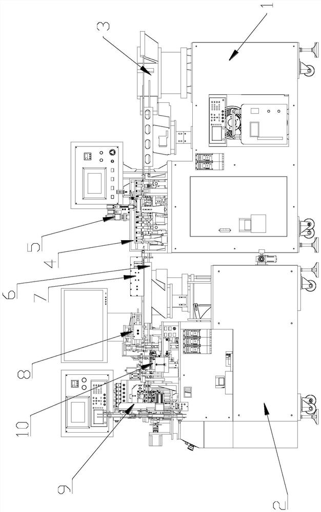
[0030] Such as Figure 1-5 As shown, a processing equipment for chip capacitors includes a printing device 1 at the front end and a lead cutting device 2 at the rear end, a transmission section 6 is arranged between the printing device 1 and the packaging device, and the transmission The section 6 is provided with a UV curing device 7 for curing printing ink for stamping;

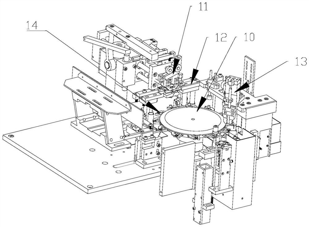
[0031] The stamping device 1 includes a feeding vibrating plate 3, a first transport module 4 and a stamping mechanism 5, the stamping mechanism 5 is arranged at the first transporting module 4, and th...


PUM


Abstract

The invention relates to chip capacitor processing equipment which comprises a stamping device located at the front end and a pin cutting device located at the rear end, a transmission section is arranged between the stamping device and the pin cutting device, and a UV curing device is arranged on the transmission section. The stamping device comprises a feeding vibration disc, a first conveying module and a stamping mechanism. The stamping mechanism is arranged at the first conveying module, the feeding vibration disc is arranged in front of the first conveying module, the pin cutting device comprises a second conveying module, a disc module, a cutter module and a discharging module, and the disc module comprises a disc body and a plurality of disc clamps. The disc clamps are evenly distributed on the outer edge of the disc body, one disc clamp is located below the tail end of the second conveying module to receive the capacitors, the cutter module is arranged on the outer side of the disc body to cut pins of the capacitors, and the discharging module is located behind the cutter module and located above the disc body. According to the invention, the integration degree is high, integrated setting of stamping and pin cutting of the capacitor is realized, and the production efficiency is effectively improved.

Description

technical field [0001] The invention relates to the technical field of capacitor production, more specifically, it relates to a processing equipment for chip capacitors. Background technique [0002] Capacitors are one of the electronic components widely used in electronic equipment, and are widely used in DC blocking, coupling, bypass, filtering, tuning loops, energy conversion and control in circuits. In the production process of capacitors, it is necessary to print relevant information on the outer surface of the capacitor, and cut off the excessively long leads of the capacitor according to the specifications of the capacitor. At present, it is necessary to use a stamping machine and a lead cutting device to complete the above process, occupying an area of The area is large, and due to the differences in the structure and production methods of the two devices, the stamping machine and the pin cutting device are not compatible, and the output end of the stamping machine c...

Claims


Application Information

Patent Timeline
Patent Type & Authority Applications(China)
IPC IPC(8): H01G13/00
CPCH01G13/00H01G13/006
Inventor 杨海铃黄瑞剑杨云飞刘福生
Owner FUJICON ELECTRONICS TECH SHAOGUAN
Why Eureka
Try Eureka