Electronic substrate and manufacturing method thereof

A technology for electronic substrates and manufacturing methods, which is applied in the fields of printed circuit manufacturing, assembly of printed circuits with electric components, and bendable/stretchable parts of circuits, etc., which can solve the problem of signal transmission efficiency, poor transmission quality, and more connections And other issues

Pending Publication Date: 2021-05-07
LENOVO (SINGAPORE) PTE LTD
View PDF1 Cites 0 Cited by
  • Summary
  • Abstract
  • Description
  • Claims
  • Application Information

AI Technical Summary

Problems solved by technology

[0004] As in the past, if FPC and two connectors are used, there will be more electrical connection parts, so it is disadvantageous in terms of signal transmission efficiency and transmission quality

Method used


Image

  • Electronic substrate and manufacturing method thereof
  • Electronic substrate and manufacturing method thereof
  • Electronic substrate and manufacturing method thereof

Examples


Embodiment Construction

[0025] Hereinafter, the electronic substrate of this embodiment will be described based on the drawings.

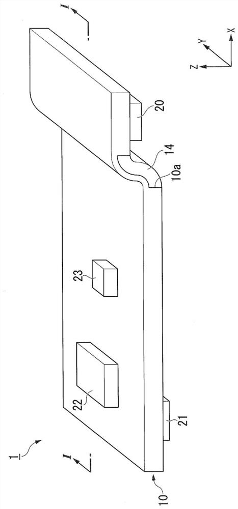
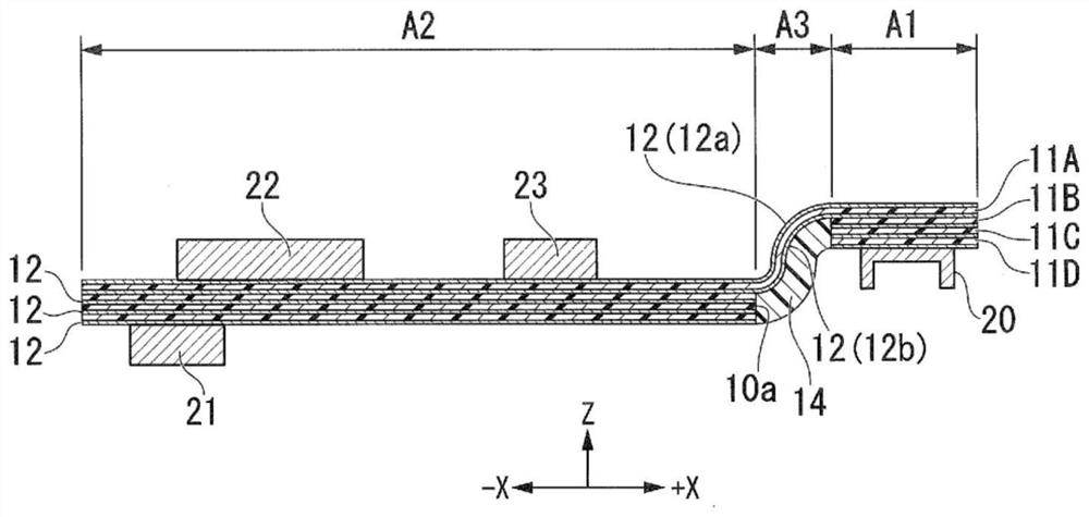
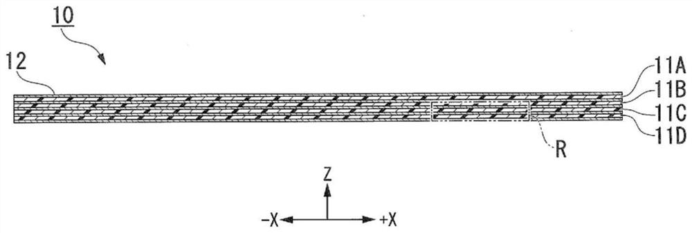
[0026] Such as Figure 1A As shown, the electronic substrate 1 is a substrate with a connector including a substrate main body 10 and a connector 20 . The substrate main body 10 may be an SSD (Solid State Drive) or a wireless communication substrate. Such as Figure 1B As shown, the substrate main body 10 is constituted by laminating a plurality of insulating layers 11A to 11D having conductive layers 12 on their surfaces. Each conductor layer 12 may be a printed circuit wiring for transmitting electrical signals, or may be a GND layer. Conductive layers 12 may be electrically connected to each other through via holes or the like. The insulating layers 11A to 11D are adhered and fixed to each other by an unillustrated adhesive layer.

[0027] The connector 20 is mounted on the board main body 10 . In addition, electronic components 21 to 23 are mounted on the substra...


PUM


Abstract

Provided is a method for manufacturing an electronic substrate or a connection substrate, with which it is possible to reduce the number of electrical connection parts. The electronic substrate (1) is provided with a substrate main body (10) configured by laminating a plurality of insulating layers (11A-11D), each of which is provided with a printed wiring on the surface thereof; a connector (20) mounted in the first region (A1) of the substrate main body (10); and at least one electronic component mounted in the second region (A2) of the substrate main body (10). Between the first region (A1) and the second region (A2) of the substrate main body (10), a third region (A3) in which a part of the insulating layers (11A-11D) are removed is formed over the entire length of the substrate main body (10) in a second direction (Y) orthogonal to the thickness direction (Z) of the substrate main body (10).

Description

technical field [0001] The present invention relates to an electronic substrate and a method for manufacturing the electronic substrate. Background technique [0002] Conventionally, in order to connect two substrates, a flexible printed circuit (FPC: Flexible printed circuit) and two connectors have been interposed. For example, in Patent Document 1, in order to connect a substrate (imaging element) to another substrate, an FPC mounted with a connector is connected to the imaging element, and a connector of the FPC is connected to a connector of a printed circuit board. [0003] Patent Document 1: Japanese Patent Laid-Open No. 2012-134816 [0004] Conventionally, if the FPC and two connectors are used, there will be many electrical connection parts, which is disadvantageous in terms of signal transmission efficiency and transmission quality. Contents of the invention [0005] The present invention has been made in consideration of such circumstances, and an object of th...

Claims


Application Information

Patent Timeline
Patent Type & Authority Applications(China)
IPC IPC(8): H05K1/02H05K1/18H05K3/00H05K3/30
CPCH05K1/0278H05K1/18H05K3/00H05K3/30H05K2203/302
Inventor 小见山博秀刘景林朱昀
Owner LENOVO (SINGAPORE) PTE LTD
Why Eureka
Try Eureka