Ion beam etching equipment and etching method thereof

A technology of ion beam etching and ion beam, which is applied in the manufacture of electrical components, semiconductor/solid-state devices, circuits, etc. It can solve the problems of not having an independent loading and unloading chamber, chip damage, and long time to establish a vacuum.

Pending Publication Date: 2021-05-04
48TH RES INST OF CHINA ELECTRONICS TECH GROUP CORP
View PDF0 Cites 1 Cited by
  • Summary
  • Abstract
  • Description
  • Claims
  • Application Information

AI Technical Summary

Problems solved by technology

However, the existing commonly used ion beam etching equipment still has the following defects: (1) it can only etch a single substrate, it cannot etch multiple substrates at the same time, and it cannot be mass-produced; (2) it does not have Independent loading and unloading chamber function, the process chamber needs to be opened every time the etching is completed, the time to establish a vacuum is long, and the effective working time is short; (3) Most of the existing ion beam etching equipment is small-sized substrate, manual scientific research equipment , does not have the functions of automatic adjustment of etching angle and online monitoring of etching film; (4) There is no temperature control device and cooling device, which cannot ensure the etching of infrared devices at lower temperatures, which may easily cause the loss of infrared devices. This is because the substrate material of infrared devices is mercury cadmium telluride. Mercury atoms are easy to escape after being bombarded by plasma and heated to a certain temperature, which will cause damage to the chip.
The existence of the above defects makes it difficult for existing ion beam etching equipment to meet the requirements of substrates (such as infrared devices) for large-scale, low-damage, and low-temperature etching processes

Method used


Image

  • Ion beam etching equipment and etching method thereof
  • Ion beam etching equipment and etching method thereof

Examples


Embodiment 1

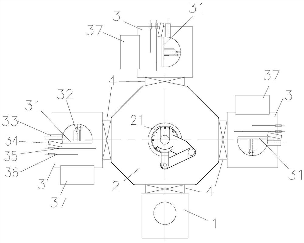
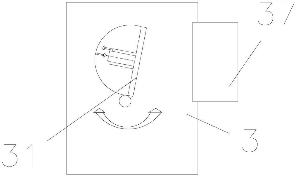
[0036] Such as figure 1 and figure 2 As shown, the ion beam etching equipment of this embodiment includes a loading and unloading chamber 1, a transport chamber 2 for transporting substrates (such as infrared devices) and at least one etching chamber 3 for etching substrates; The loading and unloading chamber 1 and the etching chamber 3 are respectively connected to the transfer chamber 2; an isolation valve 4 is provided between the loading and unloading chamber 1 and the transfer chamber 2; between the transfer chamber 2 and the etching chamber 3 An isolation valve 4 is provided; a transfer mechanism 21 for transferring substrates is provided in the transfer chamber 2 .

[0037]In the present invention, the provided loading and unloading chamber 1 is used to store different types of substrates, and a variety of different types of substrates can be placed in one loading and unloading. 1 and the transfer between the etching chamber 3, at least one etching chamber 3 is provi...


PUM


Abstract

The invention discloses ion beam etching equipment and an etching method thereof. The ion beam etching equipment comprises a substrate loading and unloading cavity, a conveying cavity used for conveying a substrate and at least one etching cavity, wherein the substrate loading and unloading cavity and the etching cavity are connected to the conveying cavity, isolation valves are arranged among the substrate loading and unloading cavity, the etching cavity and the conveying cavity, and a transfer mechanism is arranged in the conveying cavity. The etching method adopts the ion beam etching equipment to etch a substrate. The ion beam etching equipment comprises the substrate loading and unloading cavity, the conveying cavity and the at least one etching cavity; the substrate loading and unloading cavity is used for storing different types of substrates, and various different types of substrates can be placed in the substrate loading and unloading cavity through one-time loading and unloading; the conveying cavity realizes conveying of the substrates between the substrate loading and unloading cavity and the etching cavity; and the at least one etching cavity can realize simultaneous etching of a plurality of substrates. The ion beam etching equipment can meet the requirements of the substrate (such as an infrared device) on a large-size, low-damage and low-temperature etching process, can realize continuous production, improves the production efficiency, and reduces the production cost.

Description

technical field [0001] The invention relates to an ion beam etching device and an etching method thereof. Background technique [0002] Ion beam etching technology is one of the most important technologies among various etching technologies. Because it belongs to physical etching and can etch a variety of materials, it is widely used in the fields of optical components, microelectronic devices and material surface treatment. [0003] There are impurity materials on the surface of the substrate, so ion beam etching can be used to achieve material removal. For example, the contact electrode material of the mercury cadmium telluride infrared device chip is an inactive metal material such as Pt, and ion beam etching is required to realize the impurity material on the surface of the substrate. remove. However, the existing commonly used ion beam etching equipment still has the following defects: (1) it can only etch a single substrate, it cannot etch multiple substrates at the s...

Claims


Application Information

Patent Timeline
IPC IPC(8): H01L21/67H01L21/302
CPCH01L21/6704H01L21/67034H01L21/67069H01L21/6719H01L21/67213H01L21/302
Inventor 范江华胡凡龚俊刘宇黄也程文进
Owner 48TH RES INST OF CHINA ELECTRONICS TECH GROUP CORP
Why Eureka
Try Eureka