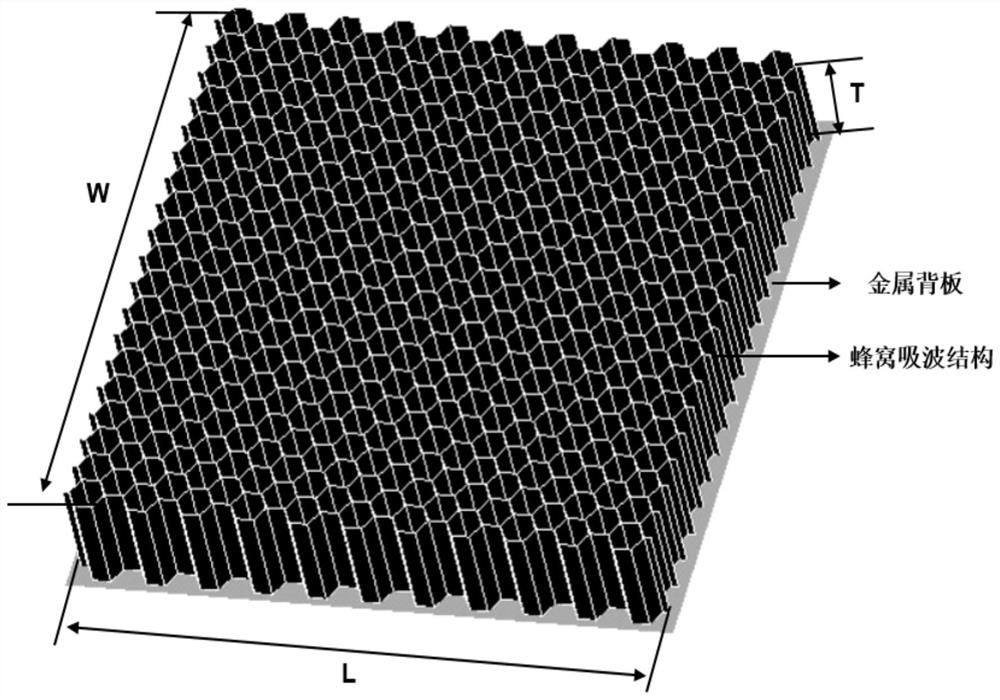
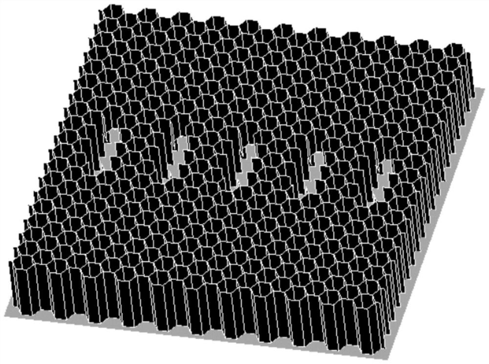
A slotted honeycomb absorbing structure
A honeycomb structure and wave structure technology, applied in the field of electronic materials, can solve the problem that the honeycomb wave absorbing structure cannot be combined with electronic components, and achieve the effect of being beneficial to energy absorption, satisfying engineering applications, and reducing the weight of the honeycomb
- Summary
- Abstract
- Description
- Claims
- Application Information
AI Technical Summary
Problems solved by technology
Method used
Image
Examples
Embodiment
[0036] Slotted honeycomb absorbing structure, its specific size parameters are (in mm): r=1.83, t0=0.1, t1=0.0125, L1=r, 2r and 3r, under each L1, the length of the lower slot W2=5 / 6*W 0 , W11, W12 and W13 are the length values of the three embodiments of the upper seam length W1, wherein W11=1 / 6*W 0 , W12=1 / 2*W 0 , W13=5 / 6*W 0 .
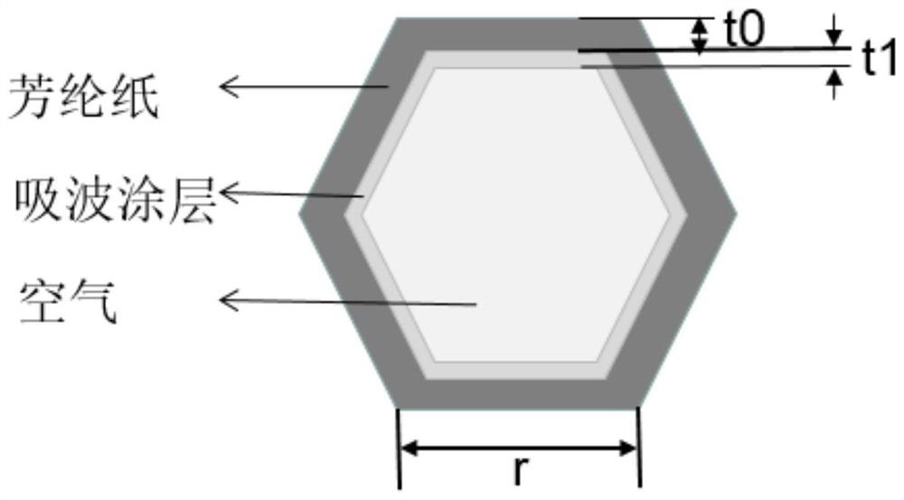
[0037]The hole wall of the honeycomb structure has two layers of material, the inner layer is aramid paper honeycomb, and the outer layer is a wave-absorbing coating. The cross-section of the aramid paper honeycomb is a regular hexagon, and the inner layer is made of a composite material made of aramid fiber paper and resin, r is the outer length of the hexagonal honeycomb hole of the aramid paper honeycomb, and t0 is the aramid paper The wall thickness of the honeycomb; the wave-absorbing coating is uniformly distributed along the axial direction of the hexagonal prism in the honeycomb hole, and its thickness is t1, such as figure 2 shown....
PUM
 Abstract
Description
Claims
Application Information
 - R&D
- Intellectual Property
- Life Sciences
- Materials
- Tech Scout
- Unparalleled Data Quality
- Higher Quality Content
- 60% Fewer Hallucinations
Browse by: Latest US Patents, China's latest patents, Technical Efficacy Thesaurus, Application Domain, Technology Topic, Popular Technical Reports.
© 2025 PatSnap. All rights reserved.Legal|Privacy policy|Modern Slavery Act Transparency Statement|Sitemap|About US| Contact US: help@patsnap.com


