An ultra-thin wafer processing device

A technology for processing equipment and wafers, which is applied to grinding equipment, metal processing equipment, manufacturing tools, etc., and can solve the problem of reducing friction between the grinding pad and the wafer, the surface roughness of the grinding pad is easy to decrease, and the side of the wafer is not easy. Fitting and fixing problems, to achieve the effect of preventing thickness inconsistency, preventing incomplete grinding, and preventing accuracy

Active Publication Date: 2022-02-18
临漳县澳皇网络科技有限公司
View PDF0 Cites 0 Cited by
  • Summary
  • Abstract
  • Description
  • Claims
  • Application Information

AI Technical Summary

Problems solved by technology

[0002] The wafer grinding device uses the friction between the wafer and the grinding pad, and with the help of the grinding liquid, the fine chips after wafer grinding follow the flow of the grinding liquid, preventing the fine chips from rubbing the wafer surface again, and making the wafer The flatness of the round surface increases, but after the friction between the wafer surface and the polishing pad, the roughness of the polishing pad surface tends to decrease, resulting in a decrease in the friction between the polishing pad and the wafer. Replacement, frequent disassembly will easily lead to loosening of the fixing device, and the thinner wafer side is not easy to be fixed, and the outer side of the wafer is easy to extend under the grinding force, which easily leads to inconsistent thickness of the outer side of the wafer, so it is easy to be damaged under the rotating grinding force. to tear

Method used


Image

  • An ultra-thin wafer processing device
  • An ultra-thin wafer processing device
  • An ultra-thin wafer processing device

Examples


Embodiment 1

[0025] Such as Figure 1-Figure 5 Shown:

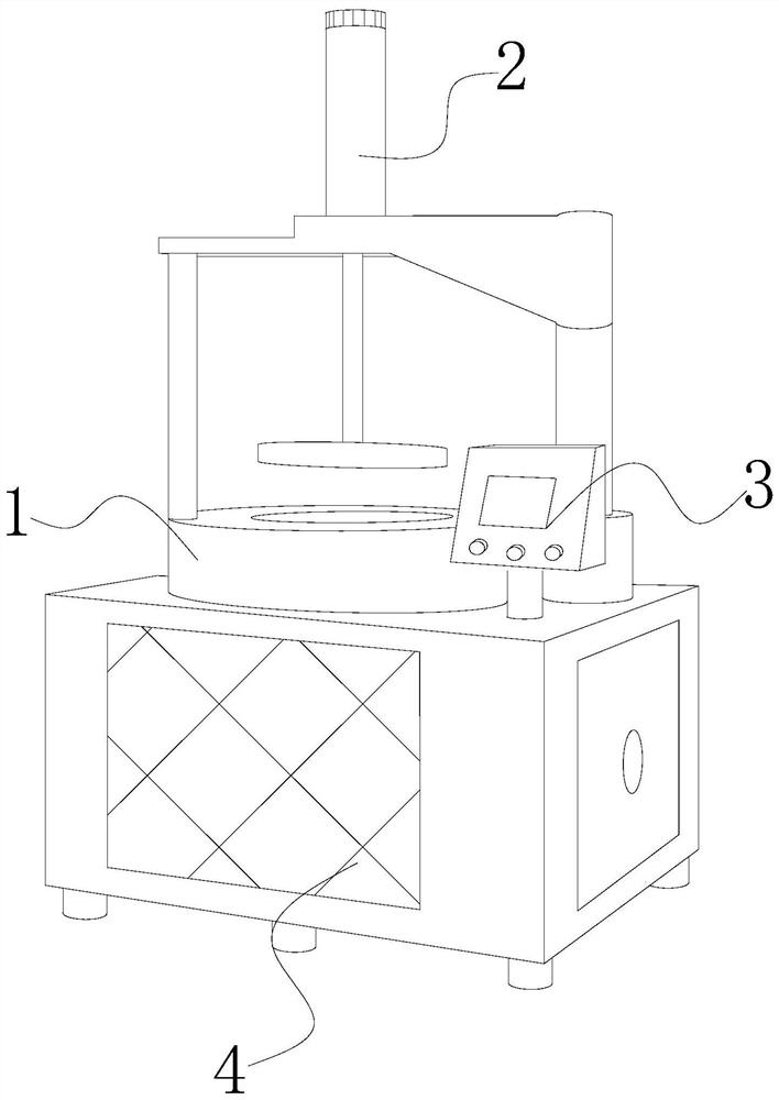
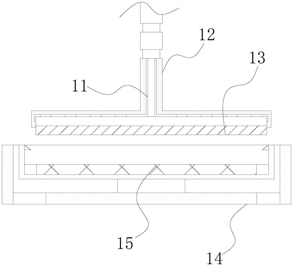
[0026] An ultra-thin wafer processing device according to the present invention, its structure includes a processing mechanism 1, a rotator 2, a control switch 3, and a workbench 4, the rotator 2 and the processing mechanism 1 are located on the same central axis, and the control switch 3 Embedded on the upper surface of the workbench 4, the processing mechanism 1 is installed on the upper end of the workbench 4, the rotator 2 is fixed on the upper end of the workbench 4, the processing mechanism 1 is provided with a fixed plate 11, a retractor 12, a grinding Structure 13, rotating plate 14, fixed structure 15, the expander 12 is embedded on the outside of the fixed plate 11, and the fixed plate 11 and the rotator 2 are located on the same central axis, the grinding structure 13 is fixedly attached to the expander 12 Inside the lower end, the lower end of the fixed plate 11 runs through the inside of the grinding structure 13, the fi...

Embodiment 2

[0033] Such as Figure 6-Figure 8 Shown:

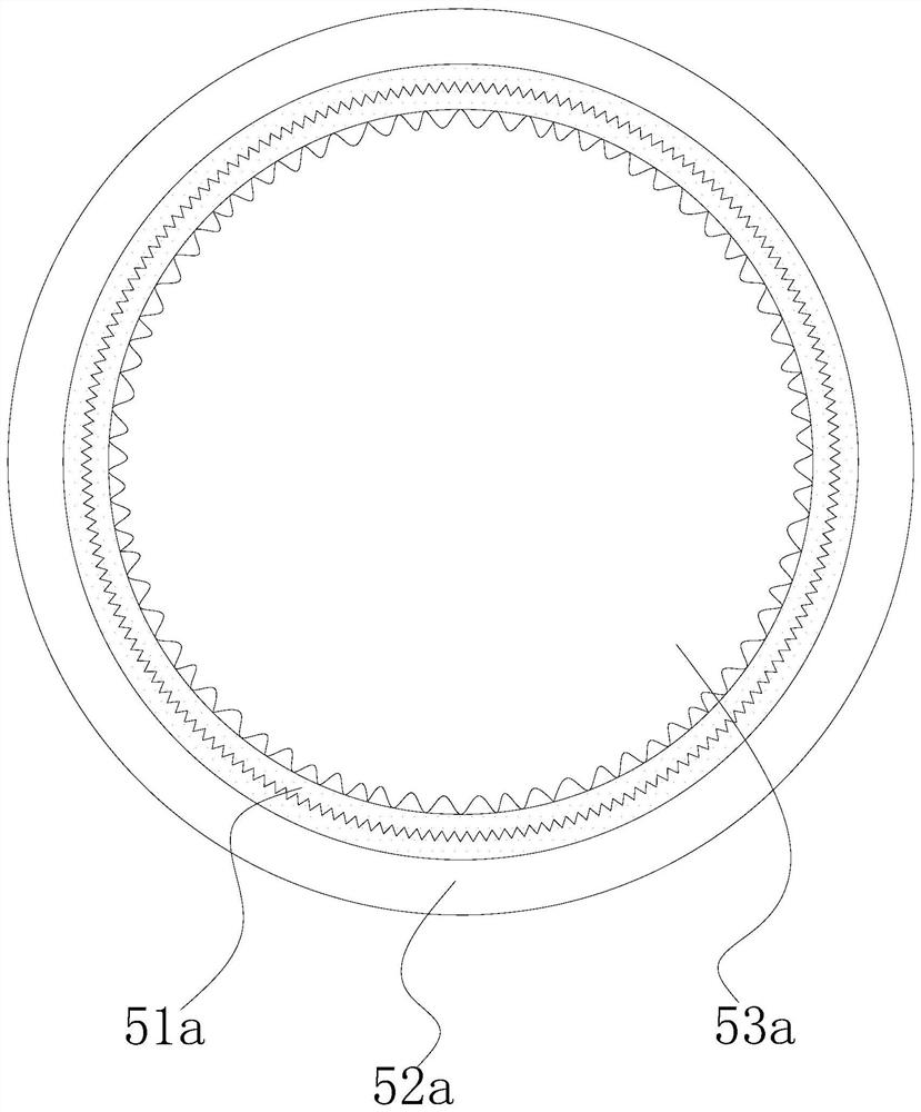
[0034]Wherein, the grinding structure 13 is provided with a grinding plate w1, a friction structure w2, an air hole w3, and a fixed ring w4, the friction structure w2 runs through the inside of the grinding plate w1, and the air holes w3 are provided with thirty The plate w1 is circularly distributed at the center point and runs through each other. The fixed ring w4 is welded on the outside of the grinding plate w1. The friction structure w2 is located on both sides of the air hole w3. The fixed ring w4 is embedded and fixed on the inner side of the lower end of the retractor 12. The friction structure w2 spreads out from the central axis of the grinding plate w1, and the diffusion becomes larger as it goes to the outside, so that the grinding plate w1 rotates to grind the wafer, and the heat generated by friction is diffused through the vent hole w3.

[0035] Wherein, the friction structure w2 is provided with a fitting plate w21, a...


PUM


Abstract

The invention discloses an ultra-thin wafer processing device, the structure of which comprises a processing mechanism, a rotator, a control switch, and a workbench. The mechanism is installed on the upper end of the workbench, and the rotator is fixed on the upper end of the workbench. The extended part of the wafer acts on the friction block. Under the reverse rotation of the wafer, it acts on the continuous bending structure of the friction block and the bending plate, causing a sticking effect on the wafer. Combined force, avoiding the extension of the outer side of the wafer while enhancing the smoothness of the outer side of the wafer, and preventing the problem of inconsistent thickness on the outer side of the wafer. After the wafer is lost, the grinding structure is controlled to lift up and down, so that the fixed ring drives the grinding plate up and down, so that the stressed structure and the sticking The plywood is exposed through the gap groove, which increases the length of the stressed structure and enhances the friction force of the arc-shaped knife edge in the support rod against the wafer, avoiding the need for frequent disassembly and replacement after grinding loss, and preventing frequent disassembly and installation from affecting the accuracy of the grinding structure.

Description

technical field [0001] The invention relates to the field of wafer coating, in particular to an ultra-thin wafer processing device. Background technique [0002] The wafer grinding device uses the friction between the wafer and the grinding pad, and with the help of the grinding liquid, the fine chips after wafer grinding follow the flow of the grinding liquid, preventing the fine chips from rubbing the wafer surface again, and making the wafer The flatness of the round surface increases, but after the friction between the wafer surface and the polishing pad, the roughness of the polishing pad surface tends to decrease, resulting in a decrease in the friction between the polishing pad and the wafer. Replacement, frequent disassembly will easily lead to loosening of the fixing device, and the thinner wafer side is not easy to be fixed, and the outer side of the wafer is easy to extend under the grinding force, which easily leads to inconsistent thickness of the outer side of ...

Claims


Application Information

Patent Timeline
Patent Type & Authority Patents(China)
IPC IPC(8): B24B37/10B24B37/34B24B27/00B24B41/00B24B37/30H01L21/304
CPCB24B37/107B24B37/34B24B27/0046B24B41/007B24B37/30H01L21/304
Inventor 赵震
Owner 临漳县澳皇网络科技有限公司
Why Eureka
Try Eureka