Semiconductor production control method and system

A production control method and production control technology, applied in the general control system, control/adjustment system, adaptive control, etc., can solve the problems of semiconductor production lines that need to be improved, so as to improve quality and efficiency, increase computing efficiency, and increase computing speed Effect

Active Publication Date: 2021-03-02
CHANGXIN MEMORY TECH INC
View PDF7 Cites 3 Cited by
  • Summary
  • Abstract
  • Description
  • Claims
  • Application Information

AI Technical Summary

Problems solved by technology

[0004] However, the effect of the existing R2R control method on improving the quality and efficiency of the semiconductor production line still needs to be improved

Method used


Image

  • Semiconductor production control method and system
  • Semiconductor production control method and system
  • Semiconductor production control method and system

Examples


Embodiment Construction

[0027] It can be known from the background art that the current semiconductor production control methods have limited effects on improving quality and performance.

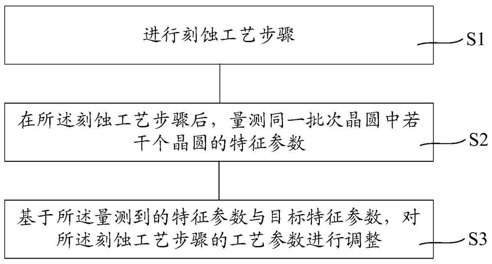
[0028] Current semiconductor control methods are based on measurement results for feedback control. figure 1 It is a schematic flowchart of a semiconductor production control method, refer to figure 1 , the semiconductor production control method includes the following steps: step S1, performing an etching process step; step S2, after the etching process step, measuring the characteristic parameters of several wafers in the same batch of wafers; step S3, based on The measured characteristic parameters and the target characteristic parameters are used to adjust the process parameters of the etching process step.

[0029] However, the above control method is less effective for adjusting the process parameters of the etching process step. The analysis found that the reasons for the limited effect of the above contr...


PUM


Abstract

The embodiment of the invention relates to a semiconductor production control method and control system, and the method comprises the steps: building a prediction model based on historical data, the prediction model being used for predicting characteristic parameters of a wafer after the second step, and the historical data comprising historical process parameters of the historical first step, historical process parameters of the historical second step and historical characteristic parameters of the wafer after the second step; after the current second step, measuring the characteristic parameters of a part of wafers in the same batch of wafers to obtain actual measurement data; on the basis of the prediction model, predicting the characteristic parameters of the remaining wafers in the same batch of wafers to obtain prediction data; and adjusting the process parameters in the second step based on the prediction data and the actual measurement data. According to the embodiment of the invention, the adjustment mechanism of process production automation can be improved.

Description

technical field [0001] The present invention relates to the technical field of semiconductors, in particular to a semiconductor production control method and control system. Background technique [0002] With the improvement of semiconductor product integration and manufacturing capacity, the semiconductor manufacturing process has become more and more complex, and the requirements for semiconductor manufacturing equipment and its control performance have become higher and higher. [0003] The semiconductor manufacturing process can be divided into five manufacturing stages, namely wafer preparation, wafer fabrication, wafer testing / picking, assembly and packaging, and final testing. The performance of the R2R (Run-to-Run) control method in the semiconductor manufacturing process affects the yield of semiconductor products, the number of re-work, and the productivity and economic benefits of the semiconductor manufacturing industry. [0004] However, the effect of the exist...

Claims


Application Information

Patent Timeline
Patent Type & Authority Applications(China)
IPC IPC(8): G05B13/04
CPCG05B13/042G05B13/048Y02P90/02
Inventor 陈振豪赖国文
Owner CHANGXIN MEMORY TECH INC
Why Eureka
Try Eureka