Composite film, preparation method and electronic component

A composite film and film technology, which is applied in the direction of electrical components, piezoelectric devices/electrostrictive devices, piezoelectric/electrostrictive/magnetostrictive devices, etc., can solve problems affecting the performance of composite films and avoid air bubbles Defects, effects of good bondability

Active Publication Date: 2021-02-26
JINAN JINGZHENG ELECTRONICS
View PDF8 Cites 3 Cited by
  • Summary
  • Abstract
  • Description
  • Claims
  • Application Information

AI Technical Summary

Problems solved by technology

[0005] In order to solve the problem that in the prior art, when the composite film is prepared by bonding the functional film layer and the silicon oxide layer, a layer of water film is formed in the bonding surface, thereby affecting the performance of the composite film

Method used


Image

  • Composite film, preparation method and electronic component
  • Composite film, preparation method and electronic component
  • Composite film, preparation method and electronic component

Examples


Embodiment Construction

[0057] In order to enable those skilled in the art to better understand the solutions of the present invention, the technical solutions in the embodiments of the present invention will be clearly and completely described below in conjunction with the drawings in the embodiments of the present invention.

[0058] The following will clearly and completely describe the technical solutions in the embodiments of the present invention with reference to the accompanying drawings in the embodiments of the present invention. Obviously, the described embodiments are only some, not all, embodiments of the present invention. Based on the embodiments of the present invention, all other embodiments obtained by those skilled in the art without creative efforts fall within the protection scope of the present invention.

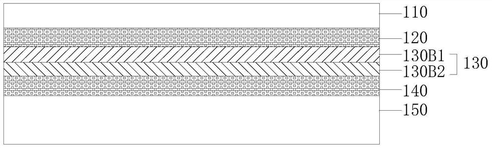
[0059] figure 1 A schematic structural view of a composite film provided in an embodiment of the present application is shown.

[0060] Such as figure 1 As shown, a composi...


PUM

PropertyMeasurementUnit
thicknessaaaaaaaaaa
thicknessaaaaaaaaaa
thicknessaaaaaaaaaa

Abstract

The invention discloses a composite film, a preparation method and an electronic component. The composite film comprises a film substrate, a first isolation layer, a bonding layer, a second isolationlayer and a support substrate which are stacked in sequence, wherein the bonding layer is formed by performing hydrophilic bonding on a first amorphous silicon layer and a second amorphous silicon layer and then performing heat treatment, and the bonding layer comprises a first silicon oxide layer and a second silicon oxide layer. Through bonding of the first amorphous silicon layer and the secondamorphous silicon layer, the composite film has good bonding capability, so that the problem that a film substrate is easy to peel off from a support substrate in the subsequent cutting process of the prepared composite film is solved. Meanwhile, water molecules exist between the first silicon oxide layer and the second silicon oxide layer, so that the water molecules between the first silicon oxide layer and the second silicon oxide layer can be diffused into the first isolation layer and the second isolation layer, and the defect that bubbles are generated in the functional film layer in the film substrate due to generation of water vapor is avoided.

Description

technical field [0001] The application belongs to the field of semiconductor element preparation, and in particular relates to a composite thin film, a preparation method and electronic components. Background technique [0002] The composite film generally includes a functional film layer, an isolation layer and a substrate layer. Among them, the material of the functional film layer generally has properties such as piezoelectricity, ferroelectricity, photoelectricity, photoelasticity, pyroelectricity, photorefraction and nonlinearity, and can be widely used It is used in various core electronic components such as surface acoustic wave devices, thin film bulk acoustic resonators, and photoelectric sensors. [0003] In the prior art, taking a functional film layer with piezoelectric properties as an example, for example, the functional film layer is a lithium tantalate film material, and the isolation layer is a silicon oxide material. The corresponding method for preparing a...

Claims


Application Information

Patent Timeline
Patent Type & Authority Applications(China)
IPC IPC(8): H01L41/08H01L41/312H10N30/00H10N30/072
CPCH10N30/072H10N30/706
Inventor 李洋洋李真宇杨超
Owner JINAN JINGZHENG ELECTRONICS
Why Eureka
Try Eureka