Detection circuit, chip and related electronic device

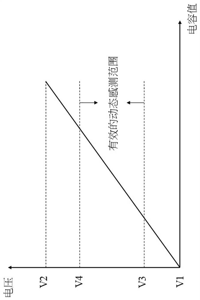
A detection circuit and circuit technology, which is applied in the direction of measuring devices, material capacitance, geophysical measurement, etc., can solve the problems of small effective sensing signal, shedding, difficult to accurately identify the back-end circuit, etc., and achieve an effective sensing range The effect of enhancing and reducing the impact

Active Publication Date: 2021-02-26
SHENZHEN GOODIX TECH CO LTD
View PDF20 Cites 0 Cited by
  • Summary
  • Abstract
  • Description
  • Claims
  • Application Information

AI Technical Summary

Problems solved by technology

This change is easily misjudged as earphone wearing, falling off, or finger touch, which leads to misoperation
[0003] In addition, in the prior art, since the capacitance detection value read by the reading circuit actually includes the capacitance value change caused by the temperature, in order to reserve the capacitance value change range caused by the temperature, the reading circuit reads The effective sensing range of the detected value is quite limited, which often leads to inaccurate judgments when judging whether there is a human body approaching based on the capacitance detection value or inaccurate judgments for other applications based on the capacitance detection value
For example, the small signal amount of the effective sensing signal makes it difficult for the back-end circuit to accurately identify the effective sensing signal

Method used


Image

  • Detection circuit, chip and related electronic device
  • Detection circuit, chip and related electronic device
  • Detection circuit, chip and related electronic device

Examples


Embodiment Construction

[0018] The following disclosure provides various implementations or illustrations, which can be used to achieve different features of the disclosure. Specific examples of components and arrangements are described below to simplify the present disclosure. It will be appreciated that these descriptions are merely examples and are not intended to limit the disclosure. For example, in the description below, forming a first feature on or over a second feature may include some embodiments wherein the first and second features are in direct contact with each other; and may also include In some embodiments, additional components are formed between the first and second features, such that the first and second features may not be in direct contact. In addition, this disclosure may reuse reference symbols and / or labels in various embodiments. Such repetition is for the sake of brevity and clarity, and does not in itself represent a relationship between the different embodiments and / or ...


PUM


Abstract

The invention discloses a detection circuit, a chip and a related electronic device. The detection circuit comprises a first input terminal, a second input terminal, an terminal end of a differentialintegral circuit, an energy storage part, a first switching circuit, a second switching circuit, a third switching circuit, a fourth switching circuit, a fifth switching circuit and a sixth switchingcircuit. The detection circuit generates a detection voltage signal according to a sensing capacitance value between the first input terminal and the second input terminal. The first switching circuitis coupled to the first input terminal, the input terminal of the differential integrating circuit and a grounding terminal. The second switching circuit is coupled to the second input terminal, theinput terminal of the differential integrating circuit and the grounding terminal. The third switching circuit is coupled to the input terminal of the differential integrating circuit and the operating voltage. The fourth switching circuit is coupled to the energy storage member and the ground terminal. The fifth switching circuit is coupled to the energy storage member, the ground terminal and the operating voltage. The sixth switching circuit is coupled to the first terminal of the energy storage component and the input terminal of the differential integrating circuit. The differential integrating circuit is used for integrating according to the voltage of the input terminal of the differential integrating circuit to generate a detection voltage signal.

Description

technical field [0001] The present application relates to a detection circuit, in particular to a self-capacitance detection circuit, a chip and related electronic devices. Background technique [0002] Electronic products often involve various human-computer interactions based on capacitance detection. For example, in earphones, capacitive in-ear detection is often used to realize the wear / off detection of the earphones to control whether the earphones perform music playback and other operations, and use capacitive touch detection to realize gestures such as click, double-click, and slide Recognition, and then complete human-computer interaction in various application scenarios; for example, touch detection or gesture recognition based on capacitive detection is also involved in mobile phones and vehicle touch controls. However, as the temperature changes, the capacitance value of the detected capacitor will also change, and this phenomenon of capacitance change due to tem...

Claims


Application Information

Patent Timeline
Patent Type & Authority Applications(China)
IPC IPC(8): G01V3/00G01N27/22
CPCG01N27/228G01V3/00
Inventor 余倩
Owner SHENZHEN GOODIX TECH CO LTD
Why Eureka
Try Eureka