IC chip appearance inspection module

A technology of appearance inspection and chips, which is applied in measuring devices, material analysis through optical means, instruments, etc., can solve the problems of inspection IC chip appearance inspection productivity cannot be improved, and the overall mechanism action increases, so as to reduce the cost of procurement and replacement , increase production capacity, and reduce the effect of up and down movements

Pending Publication Date: 2021-02-23
KING YUAN ELECTRONICS
View PDF0 Cites 0 Cited by
  • Summary
  • Abstract
  • Description
  • Claims
  • Application Information

AI Technical Summary

Problems solved by technology

[0005] As shown above, the above-mentioned existing IC chip appearance inspection module 9 can only image one IC chip 92 at a time, and is limited by the structure of the inspection module 9. After the linear transfer device 90 absorbs the IC chip 92, it needs to be moved. Position to a fixed point and then descend to the fixed point of the optical IC test seat 95 to perform imaging. After the imaging is completed, the linear transfer device 90 needs to rise and then move to another place to perform the next imaging. As a result, the inspection capacity for inspecting the appearance of IC chips cannot be increased, which is not very ideal, and there is still room for improvement

Method used


Image

  • IC chip appearance inspection module
  • IC chip appearance inspection module
  • IC chip appearance inspection module

Examples


Embodiment Construction

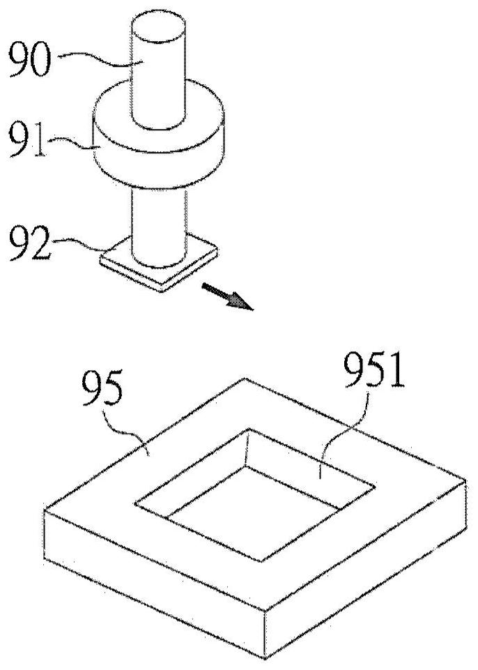
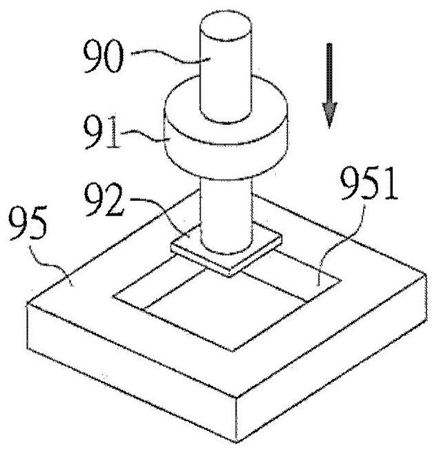
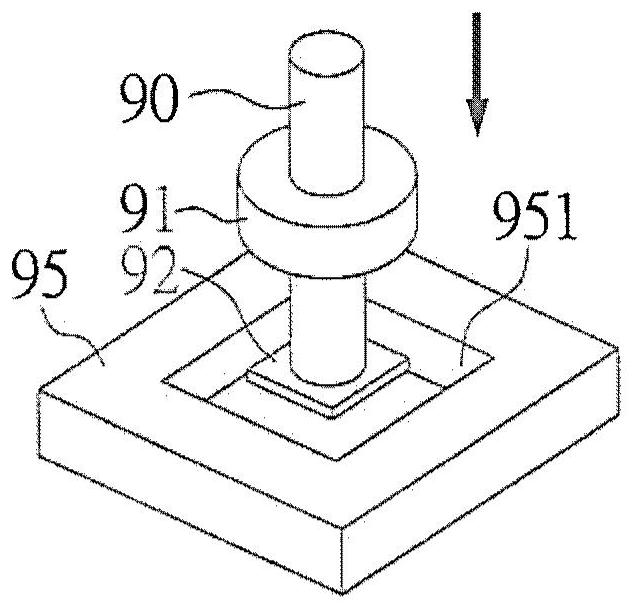
[0043] Such as figure 2 , image 3 , Figure 4 and Figure 5 As shown, they are the perspective view of the IC chip appearance inspection module of the first preferred embodiment of the present invention, the perspective view of the IC chip appearance inspection module from another perspective, the perspective view of the nozzle steering mechanism and the perspective view of the optical IC inspection seat. The IC chip appearance inspection module 1 of this embodiment includes a machine table 10 , two optical IC inspection seats 20 , an imaging module 2 , a driving device and a nozzle steering mechanism 40 .

[0044] Such as figure 2As shown, the machine table 10 has a conveying unit 11, and devices such as two optical IC inspection seats 20, an imaging module 2 and a suction nozzle steering mechanism 40 are all arranged on the machine table 10, and the two optical IC inspection seats 20 is correspondingly arranged on the machine platform 10 . In addition, the suction no...


PUM


Abstract

The invention provides an IC chip appearance inspection module. The IC chip appearance inspection module comprises a machine table, two optical IC inspection bases, an imaging module and a driving device. The machine table is provided with a conveying unit, the two optical IC inspection bases are correspondingly arranged on the machine table, and the imaging module is arranged on the machine table; and the driving device is connected with the two optical IC inspection bases, so that the distance between the two optical IC inspection bases is adjusted according to the size of the IC chip. Therefore, the distance between the two optical IC inspection bases can be quickly adjusted according to different IC chip sizes through the adjustable optical IC inspection bases, and the cost of repurchasing and replacing the optical IC inspection bases due to different IC chip sizes can be reduced and the cost of a development device can be reduced due to the fact that the whole machine table is provided with the adjustable optical IC inspection bases.

Description

technical field [0001] The invention relates to an IC chip appearance inspection module, in particular to an IC chip appearance inspection module with adjustable optical IC chip carrier distance. Background technique [0002] In the manufacturing process of semiconductor components, after the IC (Integrated Circuit Integrated Circuit) chip is manufactured and tested, it usually needs to undergo an appearance inspection before leaving the factory to ensure that the appearance of the IC chip is complete. [0003] Figure 1A-1D It is a schematic diagram of the inspection steps of the existing IC chip appearance inspection module, such as Figure 1A As shown, the IC chip appearance inspection module 9 currently on the market, its appearance inspection method is to use a linear transfer device 90 with a suction nozzle 91 to transfer an IC chip 92 to a four optical IC inspection seat 95 Above the formed inspection module, each optical IC inspection seat 95 has a reflector 951, wh...

Claims


Application Information

Patent Timeline
Patent Type & Authority Applications(China)
IPC IPC(8): G01N21/01G01N21/892
CPCG01N21/01G01N21/892
Inventor 詹勋亮梁居平王柏谚李柏勋陈家威
Owner KING YUAN ELECTRONICS
Why Eureka
Try Eureka