
Manufacturing method of figure 8 blind hole in printed circuit board

A technology of printed circuit boards and manufacturing methods, which is applied in the direction of printed circuit manufacturing, printed circuits, electrical components, etc., can solve the problems of small blind hole diameter, thin dielectric layer, separation, etc., and achieve the effect of ensuring speed

Active Publication Date: 2022-07-01
DYNAMIC ELECTRONICS KUNSHAN
View PDF5 Cites 0 Cited by
  • Summary
  • Abstract
  • Description
  • Claims
  • Application Information

AI Technical Summary

Problems solved by technology

[0002] In the traditional blind hole laser processing technology, the aperture of the laser blind hole is generally small, and the thickness of the dielectric layer is thin. For CO 2 Laser processing is easier to process; for some millimeter-wave radars, it is necessary to open irregular laser blind holes ("8"-shaped blind holes) on the PCB (printed circuit board), and the blind hole aperture and dielectric layer thickness are larger than the traditional blind hole aperture. And the thickness of the dielectric layer increases, so it brings many technical difficulties to the production
[0003] In the traditional blind hole laser processing technology, due to the small diameter of the blind hole and the thin thickness of the dielectric layer, the CO 2 Laser processing is also easy to process under the premise of meeting the quality requirements; the irregular blind hole ("8" shaped blind hole) design, there will be some overlapping areas between the two blind holes, and the traditional processing method will cause the overlapping area to be repeatedly lasered Processing causes the bottom of the blind hole to be broken down or the copper at the bottom of the blind hole is separated from the bonding sheet, so it is a technical problem in the blind hole laser processing process

Method used


Image

  • Manufacturing method of figure 8 blind hole in printed circuit board

Examples


Embodiment

[0035] Embodiment: a manufacturing method of a figure-8 blind hole in a printed circuit board, comprising the following steps:

[0036] S1. Slicing: cut the substrate plate to an appropriate size, and bake it in an oven at 120-170°C for 2-4 hours to release the internal stress of the substrate plate;

[0037] S2. Inner layer circuit: Etch the inner layer circuit. After the inner layer circuit is fabricated, scan the board surface with an optical inspection machine to ensure that there is no gap on the PAD at the bottom of the circuit / blind hole;

[0038] S3. Outer copper window: The required blind hole aperture is etched by opening the copper window. The compensation method of the copper window compensates the aperture size according to the copper thickness. When the copper thickness is 8 mil, the opening diameter of the copper window needs to be increased by 1 mil. ;

[0039] S4. Laser laser: Blind holes are burned out in the way of laser laser copper window. When the copper...


PUM


Abstract

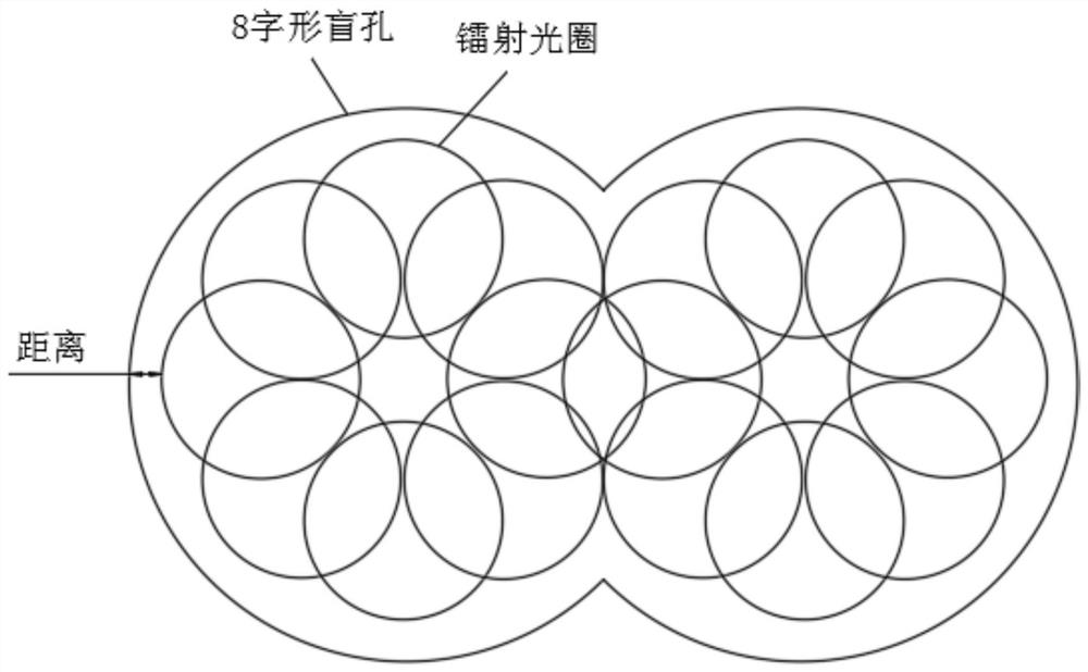
The invention discloses a method for manufacturing a figure-eight blind hole in a printed circuit board, which comprises cutting material, etching inner layer circuits, etching out the required aperture diameter of the blind hole by opening copper windows, and using laser laser copper windows to make The blind hole is burned out. When the copper window is laser processed, the size of the aperture is larger than the aperture size, and the energy will extend to the surrounding during the processing. The figure-8 blind hole is made by laser winding. The edge position of the laser aperture and the copper window The distance between the round edges is controlled between 0.5-1.0 mil. After electroplating, acid etching is performed. During the acid etching process, the blind hole area and the circuit are protected by dry film. The dry film is peeled off, the copper surface is bare and leaked for etching by the etching solution, and finally the optical inspection and resistance value test are carried out. The invention can prevent the overlapping area between the two blind holes from being repeatedly laser processed, and ensure the processing quality of the figure-eight blind holes.

Description

technical field [0001] The invention belongs to the technical field of printed circuit boards, and in particular relates to a method for manufacturing a figure-8 blind hole of a printed circuit board. Background technique [0002] In the traditional blind hole laser processing technology, the laser blind hole diameter is generally small, and the thickness of the dielectric layer is thin. 2 Laser processing is easier to process; for some millimeter-wave radars, irregular laser blind holes (“8-shaped blind holes”) need to be opened on the PCB (printed circuit board), and the blind hole aperture and the thickness of the dielectric layer are larger than the traditional blind hole aperture. And the thickness of the dielectric layer increases, so it brings many technical difficulties to the production. [0003] In the traditional blind hole laser processing process, due to the small diameter of the blind hole and the thin thickness of the dielectric layer, the CO 2 Laser process...

Claims


Application Information

Patent Timeline
Patent Type & Authority Patents(China)
IPC IPC(8): H05K3/00C25D7/00C25D3/38C23F1/18
CPCH05K3/0017H05K3/0035C25D3/38C25D7/00C23F1/18
Inventor 黄铭宏
Owner DYNAMIC ELECTRONICS KUNSHAN
Learn More