Barrier film and preparation method thereof
A technology of barrier film and film layer, applied in the field of barrier film and its preparation, can solve the problems of inability to meet the requirements of rapid development of OLED, general water vapor and oxygen isolation, and achieve excellent water vapor barrier, excellent oxygen and water vapor barrier, excellent barrier properties. The effect of the blocking effect
- Summary
- Abstract
- Description
- Claims
- Application Information
AI Technical Summary
Problems solved by technology
Method used
Image
Examples
Embodiment 1
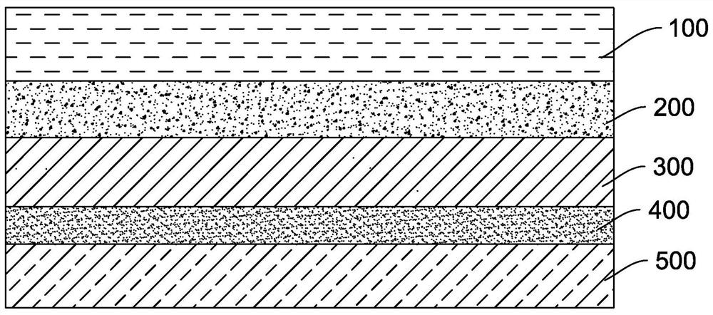
[0031] Such as figure 1 As shown, a barrier film sequentially includes a PEN film layer 100, a SPA resin layer 200, a PC film layer 300, an adhesive layer 400, and a protective film layer 500, wherein the SPA resin layer 200 is made by using OCA optical glue to bond the SPA resin It is cured between the PEN film layer and the PC film layer. The average particle size of the SPA resin is 0.5μm and the specific surface area is 5m 2 / g, the glue in the SPA resin layer 200 and the adhesive layer 400 is OCA optical glue, the protective film layer 500 is a PET release film, wherein the thickness of the PEN film layer 100 is 10 μm, and the thickness of the SPA resin layer 200 is 10 μm , the thickness of the PC film layer 300 is 15 μm, the thickness of the adhesive layer 400 is 5 μm, and the thickness of the protective film layer 500 is 15 μm.
[0032] The preparation method of above-mentioned barrier film, comprises the following steps:
[0033] (1) Apply OCA optical glue mixed with...
Embodiment 2
[0038] Compared with Example 1, the difference is that the average particle diameter of the SPA resin is 20 μm, and the specific surface area is 25 μm 2 / g, the thickness of the PEN film layer is 25 μm, the thickness of the SPA resin layer is 15 μm, the thickness of the PC film layer is 35 μm, the thickness of the adhesive layer is 10 μm, and the thickness of the protective film layer is 20 μm.
Embodiment 3
[0040] Compared with Example 1, the difference is that the average particle diameter of the SPA resin is 12 μm, and the specific surface area is 16 μm 2 / g, the thickness of the PEN film layer is 20 μm, the thickness of the SPA resin layer is 12 μm, the thickness of the PC film layer is 25 μm, the thickness of the adhesive layer is 6 μm, and the thickness of the protective film layer is 16 μm.
PUM
| Property | Measurement | Unit |
|---|---|---|
| particle size | aaaaa | aaaaa |
| specific surface area | aaaaa | aaaaa |
| thickness | aaaaa | aaaaa |
Abstract
Description
Claims
Application Information
 - R&D
- Intellectual Property
- Life Sciences
- Materials
- Tech Scout
- Unparalleled Data Quality
- Higher Quality Content
- 60% Fewer Hallucinations
Browse by: Latest US Patents, China's latest patents, Technical Efficacy Thesaurus, Application Domain, Technology Topic, Popular Technical Reports.
© 2025 PatSnap. All rights reserved.Legal|Privacy policy|Modern Slavery Act Transparency Statement|Sitemap|About US| Contact US: help@patsnap.com


