Organic compound, light-emitting element, light-emitting device, electronic apparatus, illumination device, and electronic device
A technology of organic compounds and light-emitting elements, applied in the fields of programs, products or compositions, machines, lighting devices and electronic devices, to achieve the effects of low power consumption and high luminous efficiency
- Summary
- Abstract
- Description
- Claims
- Application Information
AI Technical Summary
Problems solved by technology
Method used
Image

Examples
Embodiment approach 1
[0110]As one of materials with a low refractive index among organic compounds having carrier transport properties that can be used in organic EL elements, 1,1-bis-(4-bis(4-methyl-phenyl)-ammonia is known -Phenyl)-cyclohexane (abbreviation: TAPC). By using a material with a low refractive index for the EL layer, a light-emitting element with high external quantum efficiency can be obtained. Therefore, it can be expected that a light-emitting element with good external quantum efficiency can be obtained by using TAPC. On the other hand, TAPC has the problem of being detrimental to reliability due to its low heat resistance.
[0111]As one of the methods for obtaining a hole transport material with high heat resistance and good reliability, unsaturated hydrocarbon groups, especially cyclic unsaturated hydrocarbon groups, can be introduced into the molecule.
[0112]On the other hand, in order to obtain a material with a low refractive index, it is preferable to introduce a substituent having...
Embodiment approach 2
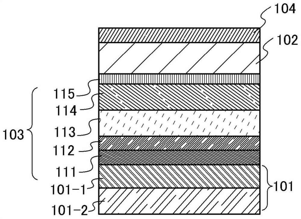
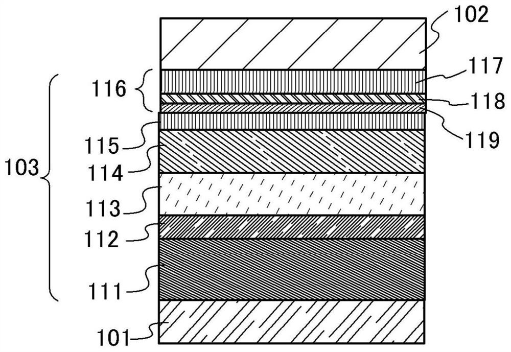
[0173]Fig. 1 shows a view of a light-emitting element according to one embodiment of the present invention. The light-emitting element of one embodiment of the present invention includes a first electrode 101, a second electrode 102, and an EL layer 103, and the organic compound described in Embodiment 1 is used for the EL layer.
[0174]The EL layer 103 includes a light emitting layer 113, and may also include a hole injection layer 111 and / or a hole transport layer 112. The light-emitting layer 113 contains a light-emitting material, and the light-emitting element of one embodiment of the present invention obtains light emission from the light-emitting material. The light-emitting layer 113 may also include a host material and other materials. The organic compound of one aspect of the present invention shown in Embodiment Mode 1 may be contained in any of the light-emitting layer 113, the hole transport layer 112, and the hole injection layer 111.
[0175]Note that although FIG. 1 shows...
Embodiment approach 3
[0235]In this embodiment mode, a light-emitting device using the light-emitting element described in Embodiment Mode 2 will be described.
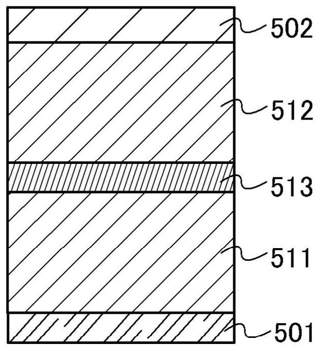
[0236]In this embodiment mode, a light-emitting device manufactured using the light-emitting element shown in Embodiment Mode 2 will be described with reference to FIG. 2. note,Figure 2A Is a top view showing the light emitting device, andFigure 2B Is alongFigure 2A A cross-sectional view cut by line A-B and line C-D in the middle. This light-emitting device includes a drive circuit section (source line drive circuit) 601, a pixel section 602, and a drive circuit section (gate line drive circuit) 603 indicated by a broken line as a unit for controlling the light emission of the light-emitting element. In addition, reference numeral 604 is a sealing substrate, reference numeral 605 is a sealing material, and the inner side surrounded by the sealing material 605 is a space 607.
[0237]Note that the guide wiring 608 is a wiring for transmitting signals ...
PUM
| Property | Measurement | Unit |
|---|---|---|
| thickness | aaaaa | aaaaa |
| thickness | aaaaa | aaaaa |
| thickness | aaaaa | aaaaa |
Abstract
Description
Claims
Application Information
 - R&D
- Intellectual Property
- Life Sciences
- Materials
- Tech Scout
- Unparalleled Data Quality
- Higher Quality Content
- 60% Fewer Hallucinations
Browse by: Latest US Patents, China's latest patents, Technical Efficacy Thesaurus, Application Domain, Technology Topic, Popular Technical Reports.
© 2025 PatSnap. All rights reserved.Legal|Privacy policy|Modern Slavery Act Transparency Statement|Sitemap|About US| Contact US: help@patsnap.com