
Pre-loading chamber and semiconductor process platform

A pre-loading and chamber technology, applied in semiconductor/solid-state device manufacturing, transportation and packaging, electrical components, etc., can solve the problem of low wafer transfer efficiency

Active Publication Date: 2020-12-29
BEIJING NAURA MICROELECTRONICS EQUIP CO LTD
View PDF7 Cites 3 Cited by
  • Summary
  • Abstract
  • Description
  • Claims
  • Application Information

AI Technical Summary

Problems solved by technology

[0004] The invention discloses a preloading chamber and a semiconductor process platform to solve the problem of low wafer transfer efficiency

Method used


Image

  • Pre-loading chamber and semiconductor process platform
  • Pre-loading chamber and semiconductor process platform
  • Pre-loading chamber and semiconductor process platform

Examples


Embodiment Construction

[0023] In order to make the purpose, technical solution and advantages of the present invention clearer, the technical solution of the present invention will be clearly and completely described below in conjunction with specific embodiments of the present invention and corresponding drawings. Apparently, the described embodiments are only some of the embodiments of the present invention, but not all of them. Based on the embodiments of the present invention, all other embodiments obtained by persons of ordinary skill in the art without making creative efforts belong to the protection scope of the present invention.

[0024] The technical solutions disclosed by various embodiments of the present invention will be described in detail below in conjunction with the accompanying drawings.

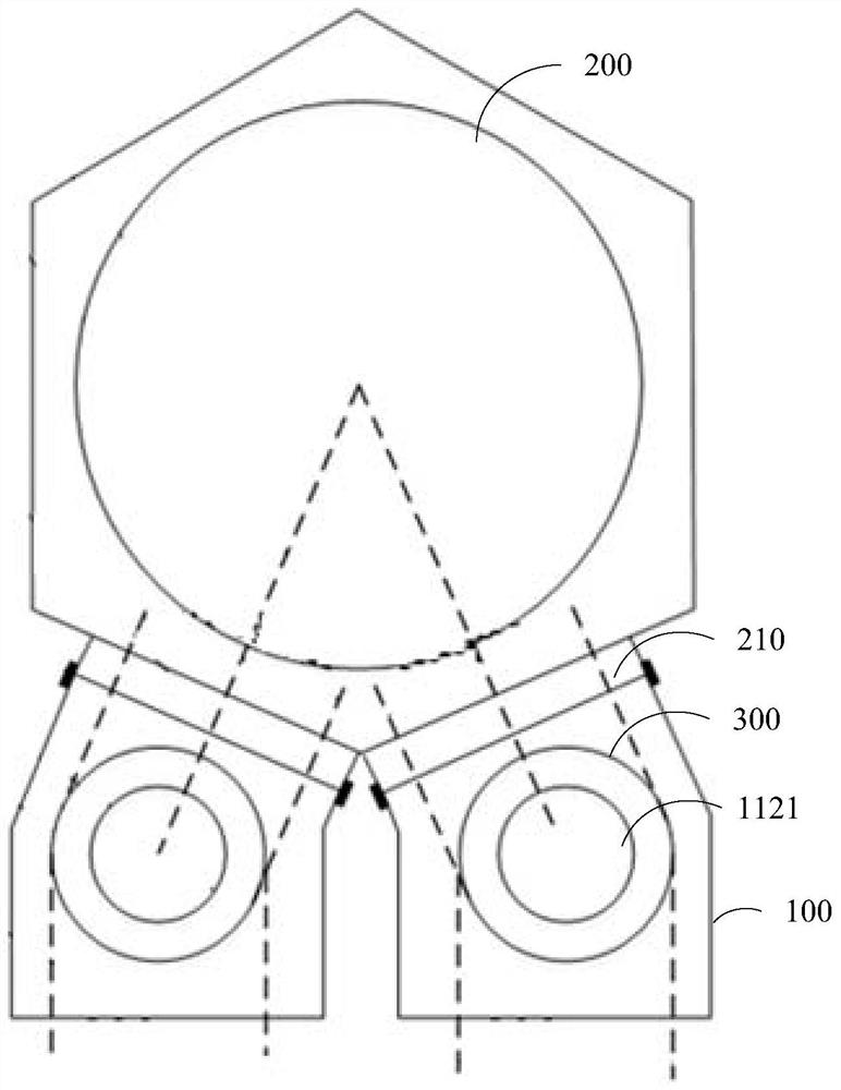
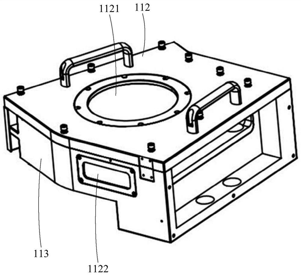
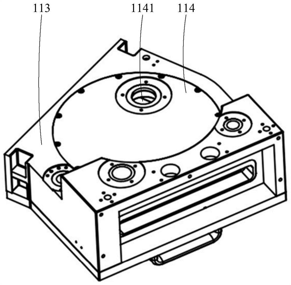
[0025] like Figure 1 to Figure 9 As shown, the embodiment of the present invention discloses a preload chamber 100 , and the disclosed preload chamber 100 includes a chamber body 110 and a waf...


PUM


Abstract

The invention discloses a pre-loading cavity and a semiconductor process platform. The pre-loading cavity comprises a chamber body and a wafer supporting frame, the chamber body is provided with an accommodating cavity, the wafer supporting frame is located in the accommodating cavity, the wafer supporting frame comprises a first bearing platform and a second bearing platform, the first bearing platform and the second bearing platform are both used for bearing wafers, the first bearing platform is arranged above the second bearing platform. The first bearing table is provided with an avoidingpart, the second bearing table is provided with a connecting part, the avoiding part and the connecting part are oppositely arranged, a fixing piece can penetrate through the avoiding part to be assembled in the connecting part, and the second bearing table is connected with the chamber body through the fixing piece. According to the scheme, the problem that the transmission efficiency of the wafer is low can be solved.

Description

technical field [0001] The invention relates to the technical field of semiconductor chip manufacturing, in particular to a preloaded chamber and a semiconductor process platform. Background technique [0002] The function of the pre-loading chamber (LOAD LOCK chamber) is a transition chamber for transferring wafers between a vacuum environment and an atmospheric environment. For example, when a wafer needs to be converted from an atmospheric environment to a vacuum environment, pre-loading The loading chamber needs to be in the atmospheric environment first, and the atmospheric manipulator can transfer the wafer into the pre-loading chamber, and then vacuumize the pre-loading chamber, so that the pre-loading chamber is in a vacuum state, and then the vacuum manipulator Transfer to the vacuum transfer chamber, and then realize the transfer of the wafer from the atmospheric environment to the vacuum environment. [0003] In the related art, the preloading chamber includes a ...

Claims


Application Information

Patent Timeline
Patent Type & Authority Applications(China)
IPC IPC(8): H01L21/677H01L21/687H01L21/67
CPCH01L21/67184H01L21/67196H01L21/67739H01L21/67742H01L21/6875H01L21/68785Y02P70/50
Inventor 马良
Owner BEIJING NAURA MICROELECTRONICS EQUIP CO LTD
Learn More