Lithographic apparatus and method for detecting pupil plane transmittance of lithographic apparatus

A technology of lithography equipment and detection methods, which is applied in the field of image sensors, can solve the problems of detection time length, etc., and achieve the effects of short detection time, guaranteed imaging contrast, and convenient detection process

Active Publication Date: 2020-12-29
SHANGHAI MICRO ELECTRONICS EQUIP (GRP) CO LTD
View PDF3 Cites 0 Cited by
  • Summary
  • Abstract
  • Description
  • Claims
  • Application Information

AI Technical Summary

Problems solved by technology

[0005] The purpose of the present invention is to provide a lithography equipment to solve the problem that the existing lithography equipment cannot realize the detection process of pupil transmittance online and the detection time is long

Method used


Image

  • Lithographic apparatus and method for detecting pupil plane transmittance of lithographic apparatus
  • Lithographic apparatus and method for detecting pupil plane transmittance of lithographic apparatus
  • Lithographic apparatus and method for detecting pupil plane transmittance of lithographic apparatus

Examples


Embodiment 2

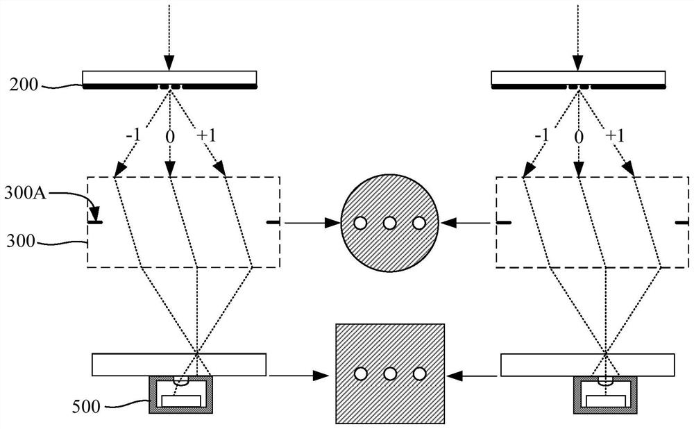
[0133] The difference from Embodiment 1 is that, in the lithography apparatus in this embodiment, the incident angle of the incident light irradiated on the phase mask can be adjusted, so that the incident light can be irradiated to the phase mask at different incident angles .

[0134] In this embodiment, the incident angle of the incident light irradiated on the phase mask can be adjusted by adjusting the light beam provided by the illumination system. Specifically, for example, the angle of the beam provided by the illumination system is deflected (that is, the beam is a deflectable beam), and then the projected beam is deflected, and the incident light irradiated on the phase mask is correspondingly deflected.

[0135] Image 6 It is a schematic diagram of the optical path when the incident light irradiated onto the phase reticle is deflected in the lithography apparatus with pupil transmittance detection function in Embodiment 2 of the present invention; Figure 7 It is...


PUM


Abstract

The invention provides a lithographic apparatus and a pupil plane transmittance detection method of the lithographic apparatus. According to a phase mask with the sub-beam energy constant, the incident energy of the corresponding sub-beam or the incident energy ratio of the sub-beam is obtained, and the detection device is also integrated in the photoetching equipment, so the detection device canbe used for obtaining the emergent energy of the sub-beam on line, and the detection result of the pupil plane transmittance can be obtained. Namely, the photoetching equipment disclosed by the invention integrates a pupil plane transmittance detection function, so the detection process can be executed on line, the detection mode is convenient, and the detection time can be effectively shortened.

Description

technical field [0001] The present invention relates to the technical field of image sensors, in particular to a lithographic equipment and a method for detecting pupil transmittance of the lithographic equipment. Background technique [0002] With the development of projection lithography technology, the performance of the projection optical system of lithography equipment has been gradually improved. At present, lithography equipment has been successfully applied in the field of integrated circuit manufacturing with submicron and deep submicron resolution. And, in order to adapt to the technological requirements of integrated circuit manufacturing breaking through 45nm, 32nm and 22nm technology nodes, lithography equipment must also improve its imaging resolution, and one of the ways to improve imaging resolution is to increase the objective lens system of lithography equipment. Numerical aperture NA, however, using an objective system with a large numerical aperture will ...

Claims


Application Information

Patent Timeline
IPC IPC(8): G03F7/20G03F1/26
CPCG03F7/70591G03F7/7085G03F1/26
Inventor 田毅强孙文凤
Owner SHANGHAI MICRO ELECTRONICS EQUIP (GRP) CO LTD
Why Eureka
Try Eureka