Wafer visual inspection equipment with removing structure and for semiconductor production

A visual inspection, semiconductor technology, applied in the direction of semiconductor/solid-state device testing/measurement, electrical components, circuits, etc., can solve problems such as not meeting the needs of use, unable to remove wafer marks, etc., to improve the efficiency of visual inspection, The effect of increasing the rotation radius and reducing damage

Inactive Publication Date: 2020-12-08
东莞市夯牛机电科技有限公司
View PDF0 Cites 0 Cited by
  • Summary
  • Abstract
  • Description
  • Claims
  • Application Information

AI Technical Summary

Problems solved by technology

[0003] The object of the present invention is to provide a wafer visual inspection device with a rejecting structure for semiconductor production, to solve the general problem in the background art that the detected wafer cannot be marked and removed, which cannot satisfy people's needs. demand problem

Method used


Image

  • Wafer visual inspection equipment with removing structure and for semiconductor production
  • Wafer visual inspection equipment with removing structure and for semiconductor production
  • Wafer visual inspection equipment with removing structure and for semiconductor production

Examples


Embodiment Construction

[0025] The technical solutions in the embodiments of the present invention will be clearly and completely described below in conjunction with the accompanying drawings in the embodiments of the present invention. Obviously, the described embodiments are only some of the embodiments of the present invention, not all of them. Based on The embodiments of the present invention and all other embodiments obtained by persons of ordinary skill in the art without making creative efforts belong to the protection scope of the present invention.

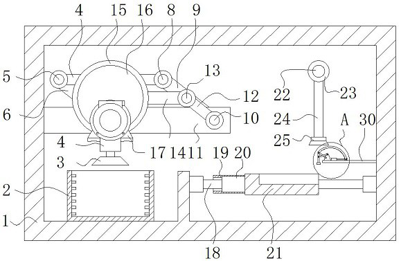
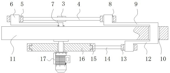
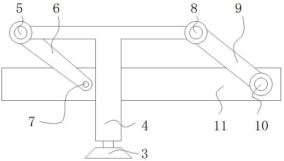
[0026] see Figure 1-5, the present invention provides a technical solution: a wafer visual inspection device with a rejecting structure for semiconductor production, including a frame 1, a feed box 2 is arranged on the lower left side of the inside of the frame 1, and a feed box 2 is arranged above the feed box 2 There is a suction cup 3, the distance from the bottom of the suction cup 3 to the top of the feeding box 2 is 2 cm, and the vertical...


PUM


Abstract

The invention discloses wafer visual inspection equipment with a removing structure and for semiconductor production. The equipment comprises a frame, wherein a feeding box is arranged on the left side of the lower part in the frame, a first connecting plate is welded above a sucker, a first connecting rod is screwed below a first lock pin, a third lock pin is screwed on the right side of the first connecting plate, and a fourth lock pin is screwed below a second connecting rod. According to the wafer visual inspection equipment with the removing structure and for semiconductor production, compared with existing common visual inspection equipment, a marking block is arranged, an air cylinder drives a fifth connecting rod to move through an air rod, and the fifth connecting rod is in an arcshape, so that the moving range of the fifth connecting rod is reduced; and the fifth connecting rod drives the marking block on a rotating rod to do circular motion with a seventh lock pin on the right side of a sixth connecting rod as the circle center through a tenth lock pin, marking removing operation is conducted, the sixth connecting rod can reduce the rotating radius of the rotating rod,and the marking removing efficiency of the equipment is improved.

Description

technical field [0001] The invention relates to the technical field of wafer visual detection, in particular to a wafer visual detection device with a rejecting structure for semiconductor production. Background technique [0002] With the progress of society, the development of economy, and the continuous improvement of science and technology, semiconductors are the last to enter every household. Home appliances, digital products, electronic products, etc. are inseparable from semiconductors. During the production of semiconductors, semiconductor wafers need to be processed. Visual inspection, the performance of the semiconductor can only be guaranteed after passing the visual inspection of the wafer. The current wafer visual inspection equipment cannot perform marking and removal operations on the inspected wafers, which cannot well meet people's needs. In view of the above situation, technological innovation is carried out on the basis of existing visual inspection equipm...

Claims


Application Information

Patent Timeline
IPC IPC(8): B07C5/36B07C5/02B07C5/34H01L21/66
CPCB07C5/02B07C5/34B07C5/362H01L22/12
Inventor 陈奕傧胡展铭陈咏诗
Owner 东莞市夯牛机电科技有限公司
Why Eureka
Try Eureka