
A gan device hardened against single event radiation

An anti-single-event radiation and device technology, applied in semiconductor devices, electrical components, circuits, etc., can solve the problem of low single-event burnout threshold voltage, and achieve the effects of alleviating avalanche breakdown, reducing bending, and increasing threshold voltage.

Active Publication Date: 2022-04-12
HANGZHOU DIANZI UNIV
View PDF4 Cites 0 Cited by
  • Summary
  • Abstract
  • Description
  • Claims
  • Application Information

AI Technical Summary

Problems solved by technology

However, the existing GaN power devices suffer from the problem that the single event burnout threshold voltage is too low

Method used


Image

  • A gan device hardened against single event radiation
  • A gan device hardened against single event radiation
  • A gan device hardened against single event radiation

Examples


Embodiment Construction

[0020] The following will clearly and completely describe the technical solutions in the embodiments of the present invention with reference to the accompanying drawings in the embodiments of the present invention. Obviously, the described embodiments are only some, not all, embodiments of the present invention. Based on the embodiments of the present invention, all other embodiments obtained by persons of ordinary skill in the art without making creative efforts belong to the protection scope of the present invention.

[0021] In order to make the above objects, features and advantages of the present invention more comprehensible, the present invention will be further described in detail below in conjunction with the accompanying drawings and specific embodiments.

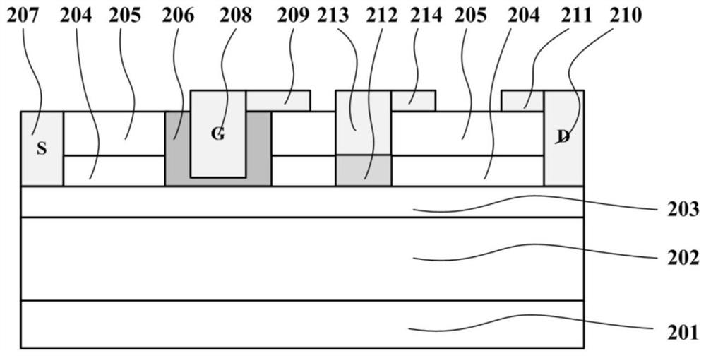
[0022] refer to figure 1 As shown, this embodiment provides a GaN device resistant to single-event radiation hardening, including a substrate 201, a buffer layer 202, a channel layer 203, a barrier layer 204, and ...


PUM

PropertyMeasurementUnit
thicknessaaaaaaaaaa

Abstract

The invention discloses a GaN device resistant to single-event radiation hardening, which comprises a substrate, a buffer layer, a channel layer, a barrier layer, and a passivation layer sequentially stacked from bottom to top; the GaN device resistant to single-event radiation hardening The two ends are respectively provided with source and drain; the source and drain penetrate through the barrier layer and passivation layer; there is a groove between the source and drain, and the groove penetrates through the barrier layer and passivation layer; the groove There is a gate inside, and a gate dielectric layer is set between the gate and the inner wall of the trench; the top of the gate and the drain are respectively connected with a gate field plate and a drain field plate; there is also a buried N well on the barrier layer, and the buried N The thickness of the well is the same as that of the barrier layer, and there is a gap between the buried N well and the trench; the top of the buried N well is connected to a Schottky electrode, and the Schottky electrode has the same width as the buried N well and is set up and down correspondingly. There is a Schottky electrode field plate on top of the electrode. The invention can prevent devices from being burned under low drain bias voltage, and effectively improves the threshold voltage of single event burning of GaN devices.

Description

technical field [0001] The invention relates to the technical field of semiconductors, in particular to a single-event radiation-resistant GaN device. Background technique [0002] GaN, a wide bandgap semiconductor material, has natural advantages in anti-irradiation applications. Due to the polarization effect, GaN can form a two-dimensional electron gas (2DEG, Two-dimensional electron gas), so that GaN devices can obtain extremely low on-resistance, and because GaN materials have extremely high critical breakdown electric field strength, the breakdown voltage of GaN devices is also higher than other semiconductor materials. Because of its high power, high frequency and other characteristics, GaN has become one of the most potential power electronic devices. [0003] As the application fields of GaN devices become wider and wider, the research on GaN in the field of radiation resistance is also gradually in-depth. Many research institutions at home and abroad have conduct...

Claims


Application Information

Patent Timeline
Patent Type & Authority Patents(China)
IPC IPC(8): H01L29/78H01L29/08H01L29/40H01L29/47
CPCH01L29/404H01L29/405H01L29/475H01L29/0847H01L29/7839
Inventor 王颖程有忠曹菲包梦恬于成浩
Owner HANGZHOU DIANZI UNIV
Learn More