PCB defect automatic detection method based on deep learning
An automatic detection and deep learning technology, applied in image data processing, instruments, character and pattern recognition, etc., can solve the problems of low efficiency and low precision, achieve high fault detection rate, save labor costs, improve reliability and efficiency sexual effect
- Summary
- Abstract
- Description
- Claims
- Application Information
AI Technical Summary
Problems solved by technology
Method used
Image

Examples
Embodiment
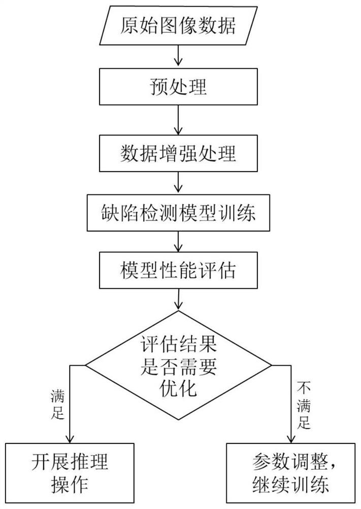
[0032] Such as figure 1 As shown, a method for automatic detection of PCB faults based on deep learning, the steps are as follows:
[0033] (1) Preprocess the original data, convert the data format and size, and complete the data set division;
[0034] Firstly, the PCB image is cropped into 600×600 sub-images, and then the data set format is converted into a unified data input format for the TensorFlow interface, and then the data set is divided into two parts: training and inference. Among them, the training data set contains 8250 images, and the test data set contains 2102 images.
[0035] (2) Carry out data enhancement processing on the preprocessed image;
[0036] Purpose of data augmentation:
[0037] 1) Expand the training samples to reduce the risk of over-fitting of the parameters of the neural network;
[0038] 2) Reduce the cost of collection, the number of PCBs with defects is small, and the collection cycle is long;
[0039] The present invention adopts six tr...
PUM
 Abstract
Description
Claims
Application Information
 - Generate Ideas
- Intellectual Property
- Life Sciences
- Materials
- Tech Scout
- Unparalleled Data Quality
- Higher Quality Content
- 60% Fewer Hallucinations
Browse by: Latest US Patents, China's latest patents, Technical Efficacy Thesaurus, Application Domain, Technology Topic, Popular Technical Reports.
© 2025 PatSnap. All rights reserved.Legal|Privacy policy|Modern Slavery Act Transparency Statement|Sitemap|About US| Contact US: help@patsnap.com