VCSEL chip and manufacturing method thereof

A manufacturing method and chip technology, applied in laser parts, electrical components, lasers, etc., can solve problems such as poor beam quality

Inactive Publication Date: 2020-10-23
江西铭德半导体科技有限公司
View PDF8 Cites 4 Cited by
  • Summary
  • Abstract
  • Description
  • Claims
  • Application Information

AI Technical Summary

Problems solved by technology

[0006] The object of the present invention is to provide a kind of VCSEL chip and its manufacturing method, to solve the problem that the light beam quality deteriorates when working at high power

Method used


Image

  • VCSEL chip and manufacturing method thereof
  • VCSEL chip and manufacturing method thereof
  • VCSEL chip and manufacturing method thereof

Examples


example 1

[0049] For the VCSEL chip that emits light at a wavelength of 940nm, a three-quantum well structure is used, and the DBR is a periodic material composed of GaAs with a quarter optical thickness and Al0.90GaAs with a quarter optical thickness. P-DBR (that is, p Type DBR layer 13) has 16 pairs of pairs, and N-DBR (that is, n-type DBR layer 11) has 38 pairs of pairs. Wherein, the material composition of the optical absorption layer 18 is In(x)GaAs, where x=0.12, the thickness is 66 nm, the diameter of the mesa 16 is 35 μm, the inner diameter of the optical absorption layer 18 is 5 μm, and the pore diameter of the oxide ring 17 is 10 μm.

example 2

[0051] For the VCSEL chip with a wavelength of 940nm for emitting light, the composition of the material of the optical absorption layer 18 is In(x)GaAs, where x=0.11, and the thickness range is 32-96nm, corresponding to λ / (8n)-3λ / (8n ), where n is the material refractive index of the absorbing layer material In0.11GaAs at a wavelength of 940, which is approximately equal to 3.65.

example 3

[0053] For the VCSEL chip with a wavelength of 905nm for emitting light, the composition of the material of the optical absorption layer 18 is In(x)GaAs, where x needs to be greater than 0.055 to ensure that the band gap of the In(x)GaAs material is smaller than the photon corresponding to the wavelength of 905nm energy. In this example, take x=0.06, the thickness of the optical absorption layer 18 is 31-93nm, corresponding to λ / (8n)-3λ / (8n), where n is the absorption layer material In0.06GaAs at wavelength 905 The refractive index of the material, approximately equal to 3.66.

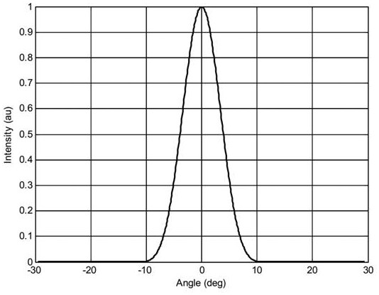
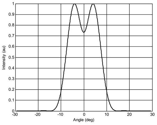
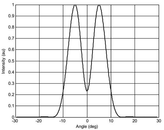
[0054] In addition, in order to further illustrate the suppression effect of the optical absorption layer 18 on high-order modes, the threshold current and light output power of the VCSEL chip in different situations were calculated, and the results are shown in Table 1. The calculation example in Table 1 is for a VCSEL with a wavelength of emitted light of 940nm For the chip, the pore diameter of the...


PUM

PropertyMeasurementUnit
Wavelengthaaaaaaaaaa
Thicknessaaaaaaaaaa

Abstract

The invention provides a VCSEL chip and a manufacturing method thereof. The VCSEL chip comprises a chip main body. The chip main body comprises an n-type DBR layer, an active region and a p-type DBR layer which are sequentially stacked from bottom to top; an oxidation ring is arranged between the p-type DBR layer and the active region; and the top of the p-type DBR layer is provided with an upperelectrode, the top of the upper electrode is provided with an optical absorption layer, the optical absorption layer is made of In(x)GaAs material, wherein x represents the molar component content ofIn, and the band gap of the optical absorption layer is smaller than the photon energy corresponding to the working wavelength of the VCSEL chip. The problem that the light beam quality becomes poor during high-power work can be solved.

Description

technical field [0001] The invention relates to the technical field of semiconductor lasers, in particular to a VCSEL chip and a manufacturing method thereof. Background technique [0002] The full name of VCSEL is Vertical Cavity Surface Emitting Laser (Vertical Cavity Surface Emitting Laser), referred to as surface-emitting laser, also known as VCSEL chip. Unlike traditional edge-emitting lasers, the laser emission direction of VCSEL is perpendicular to the substrate surface. VCSEL chips have the characteristics of low threshold current, surface emission, high luminous efficiency, extremely low power consumption, good beam quality, easy fiber coupling, ultra-narrow line width, extremely high beam quality, high polarization ratio and low cost, etc., and are widely used In laser display, information storage, laser communication, optical sensing and other fields. [0003] Among them, VCSEL chips are generally formed by epitaxial growth on substrate materials (such as GaAs). ...

Claims


Application Information

Patent Timeline
IPC IPC(8): H01S5/065H01S5/183
CPCH01S5/0653H01S5/183H01S5/18302
Inventor 仇伯仓李春勇舒凯徐化勇冯欧
Owner 江西铭德半导体科技有限公司
Why Eureka
Try Eureka