A kind of preparation method and device of indium antimonide single crystal
The technology of indium antimonide single crystal and indium antimonide seed crystal is applied in the field of preparation of indium antimonide single crystal, which can solve the problem of extremely high technical experience requirements of crystal pulling workers, unfavorable growth of large-sized single crystal, complicated crystal growth process, etc. It can avoid the risk of hydrogen explosion, the quality is stable and controllable, and the difference in carrier concentration and electron mobility is small.
- Summary
- Abstract
- Description
- Claims
- Application Information
AI Technical Summary
Problems solved by technology
Method used
Image
Examples
Embodiment 1
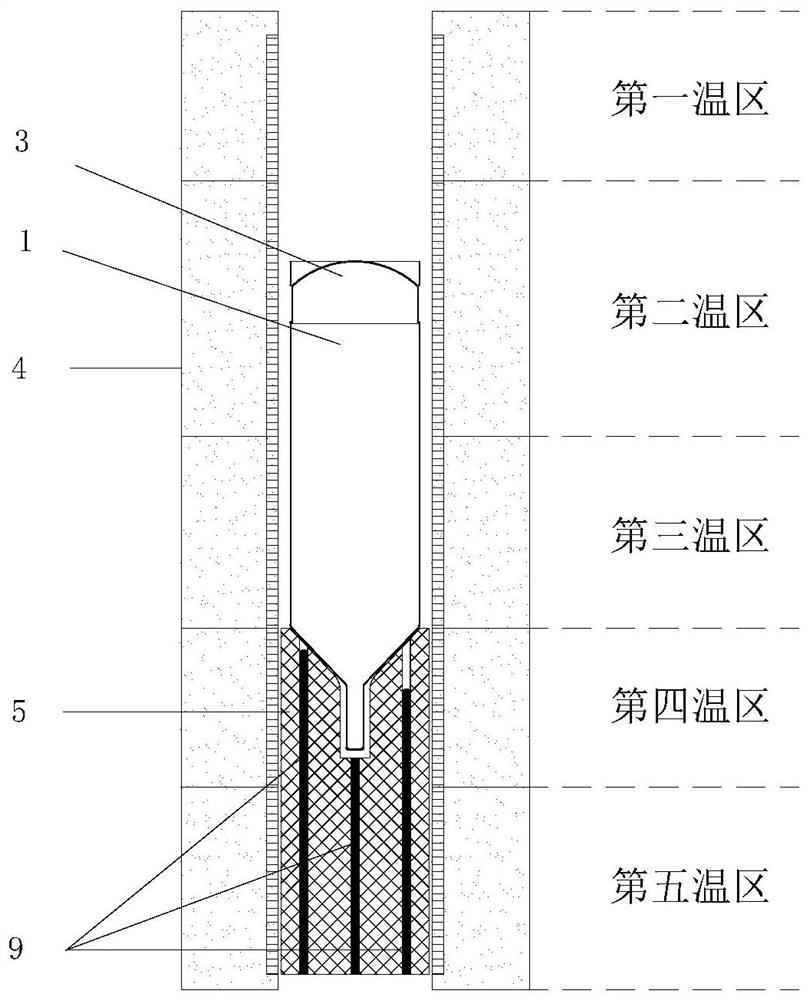
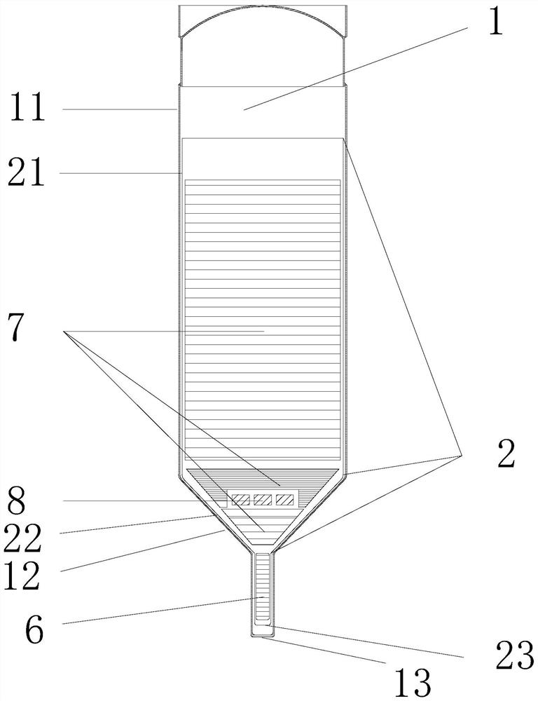
[0047] This example is an embodiment of the preparation device for indium antimonide single crystal of the present invention. For the specific structure of the preparation device, see figure 1 and figure 2 .
[0048] The preparation device comprises an airtight container, a heater 4 and a supporting device 5, wherein the airtight container includes a first crucible 1, a second crucible 2 and a sealing cap 3, the upper end of the second crucible 2 is open and placed in the first crucible 1, sealed The cap 3 is welded to the upper end of the first crucible 1, the first crucible 1 is inside the heater 4, and the supporting device 5 is used to support and fix the first crucible 1 at the lower part of the first crucible 1; the second crucible 2 includes a The main body 21, the seed crystal cavity 23 and the conical shoulder 22 connecting the main body 21 and the seed crystal cavity 23, wherein the height of the main body 21 is 230 mm, the height of the conical shoulder 22 is 50 m...
Embodiment approach
[0051] This example is an embodiment of the method for preparing an indium antimonide single crystal of the present invention. The preparation method uses the device in Example 1 to prepare an indium antimonide single crystal, and it includes the following steps:
[0052] (1) Feeding: put the second crucible 2 in the first crucible 1, and then place the indium antimonide seed crystal 6 in the direction with a dislocation density of 0 in the seed crystal chamber 23 of the second crucible. The crystal diameter is 10 mm, and the length is 50 mm. Then, 8 kg indium antimonide polycrystal 7 and 20 g diboron trioxide 8 are filled in the second crucible 2. The positional relationship of each raw material after charging is as follows: figure 2 As shown (part of the indium antimonide polycrystalline 7 has a drilled hole inside, and diboron trioxide 8 is placed in the drilled hole), immediately afterwards the air inside the first crucible 1 is evacuated, and the top is sealed with a sea...
Embodiment 3
[0056] This example is an embodiment of the method for preparing an indium antimonide single crystal of the present invention. The preparation method uses the device in Example 1 to prepare an indium antimonide single crystal, and it includes the following steps:
[0057] (1) Feeding: put the second crucible 2 in the first crucible 1, and then place the indium antimonide seed crystal 6 in the direction with a dislocation density of 0 in the seed crystal chamber 23 of the second crucible. The crystal diameter is 10mm, and the length is 50mm. Then, in the second crucible 2, 10kg of indium antimonide polycrystal 7 and 50g of boron trioxide 8 are filled. The positional relationship of each raw material after charging is as follows: figure 2 As shown (part of the indium antimonide polycrystalline 7 has a drill hole inside, and diboron trioxide 8 is placed in the drill hole), immediately after that, the air inside the first crucible 1 is evacuated, and the top is sealed with a seal...
PUM
| Property | Measurement | Unit |
|---|---|---|
| thickness | aaaaa | aaaaa |
| thickness | aaaaa | aaaaa |
| thickness | aaaaa | aaaaa |
Abstract
Description
Claims
Application Information
 - R&D Engineer
- R&D Manager
- IP Professional
- Industry Leading Data Capabilities
- Powerful AI technology
- Patent DNA Extraction
Browse by: Latest US Patents, China's latest patents, Technical Efficacy Thesaurus, Application Domain, Technology Topic, Popular Technical Reports.
© 2024 PatSnap. All rights reserved.Legal|Privacy policy|Modern Slavery Act Transparency Statement|Sitemap|About US| Contact US: help@patsnap.com


