Semiconductor MPS diode with reduced current-crowding effect and method of manufacturing same

A diode and semiconductor technology, which is applied in the field of semiconductor fusion PN-Schottky diodes, can solve the problems of local electrothermal runaway, MPS device failure, and the inability to ensure rapid diffusion of bipolar conduction current.

Pending Publication Date: 2020-09-29
STMICROELECTRONICS SRL
View PDF0 Cites 0 Cited by
  • Summary
  • Abstract
  • Description
  • Claims
  • Application Information

AI Technical Summary

Problems solved by technology

[0012] even though figure 2 and image 3 The cell-like layout of the solution allows avoiding current crowding at the corners of the device, but the applicant has found that a small local imbalance in current or temperature of one of the JB element 9 or the Schottky diode 12 can lead to local electrothermal runaway, which may cause failure of the MPS device
Furthermore, the presence of several bipolar cells does not ensure rapid diffusion of bipolar conduction current over the entire PN junction surface, even if provided with dedicated ohmic contacts 9"

Method used


Image

  • Semiconductor MPS diode with reduced current-crowding effect and method of manufacturing same
  • Semiconductor MPS diode with reduced current-crowding effect and method of manufacturing same
  • Semiconductor MPS diode with reduced current-crowding effect and method of manufacturing same

Examples


Embodiment Construction

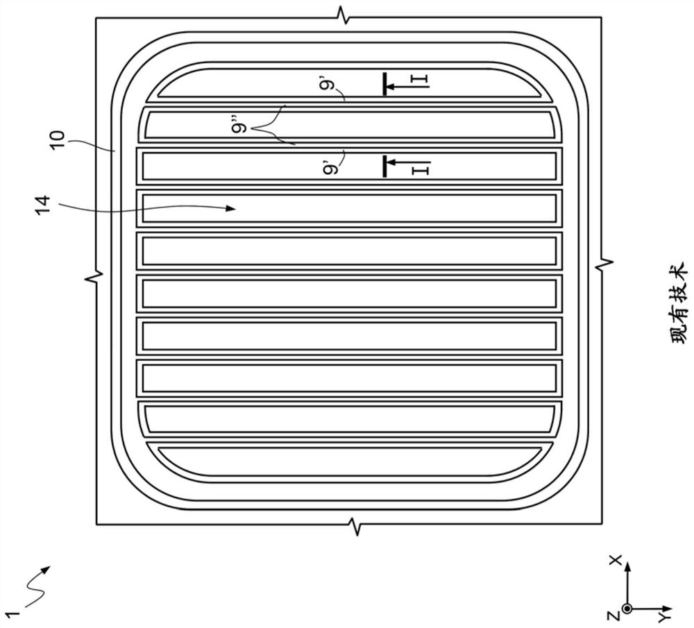
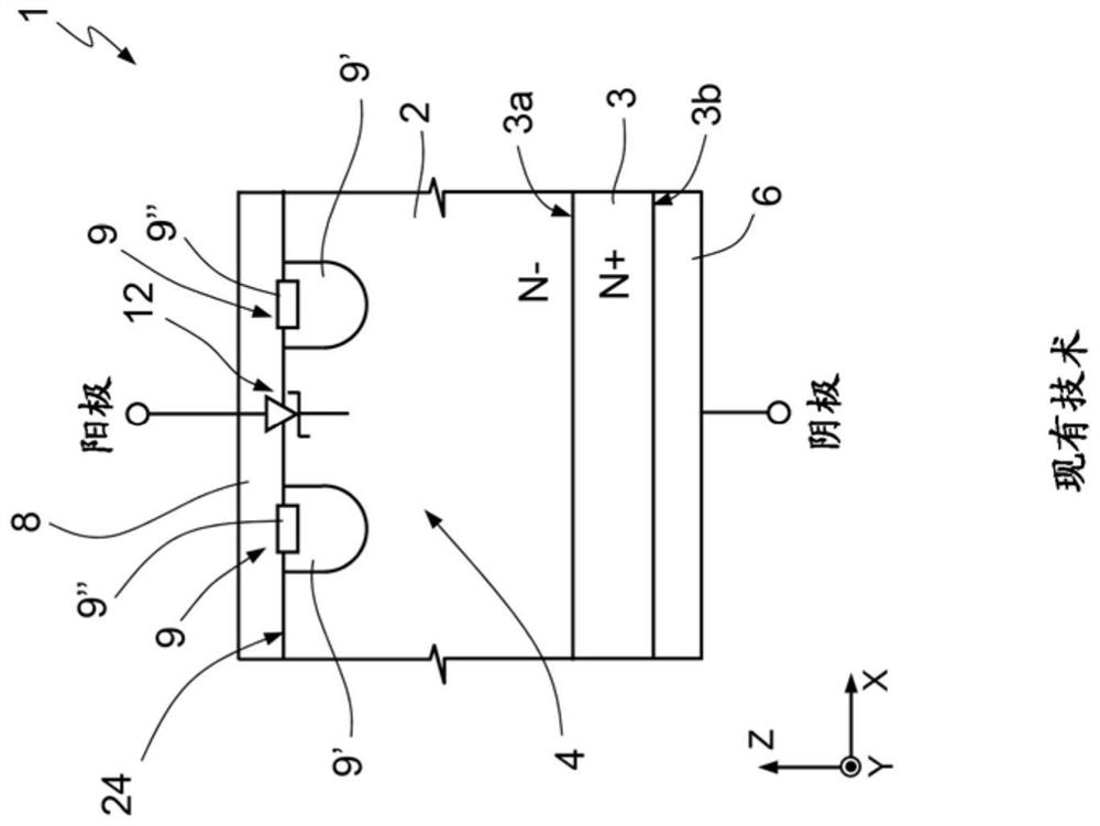
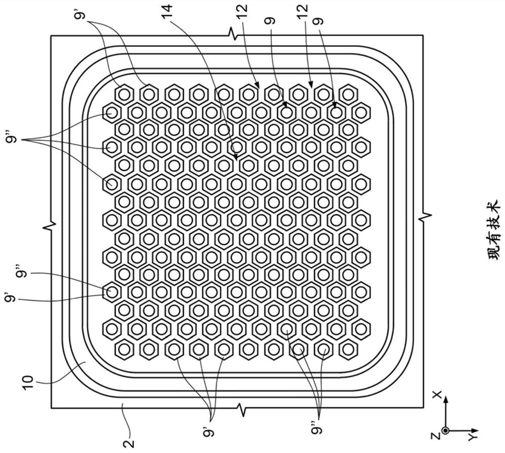
[0024] exist Figure 1A-Figure 3 In the same reference frame of the X, Y, Z axes, Figure 4A A top view (ie, on the XY plane) of a fused PN-Schottky (in particular, MPS) device 30 according to one embodiment of the present invention is shown. Figure 4B shows the same frame of reference along the Figure 4A A transverse sectional view taken along the line IV-IV. In order to improve the Figure 4A understanding that the anode metallization is not shown, but is present, as per the Figure 4B The figure is obvious.

[0025] Figure 4B A transverse cross-section (i.e., on the XZ plane) of is essentially the same as Figure 1B The transverse cross-sectional view is consistent. Similar elements are identified with the same reference numerals and will not be described in detail again.

[0026] However, when considering Figure 4A In the top view of , those skilled in the art can understand that each Schottky diode 32 in the plurality of Schottky diodes 32 includes a correspo...


PUM

PropertyMeasurementUnit
electrical resistivityaaaaaaaaaa

Abstract

Embodiments of the present disclosure relate to a semiconductor MPS diode with reduced current crowding effect and a method of manufacturing the same. A fused PN-Schottky (MPS) diode includes an N substrate, an N-drift layer, a P-doped region in the drift layer, an ohmic contact on the P-doped region, a plurality of cells within the P-doped region and being part of the drift layer without the P-doped region, and an anodic metallization on the ohmic contact and on the cells to form a junction barrier contact and a Schottky contact, respectively. The P-doped region has a grid-shaped layout thatseparates each cell from each other and together with the cells defines an active region of the MPS diode. Each cell has the same geometry among a quadrangle, a quadrangle having rounded corners, anda circle, and the ohmic contact extends continuously along the layout of the grid shape at the doped region.

Description

technical field [0001] The present disclosure relates to a semiconductor fused PN-Schottky (MPS) diode with reduced current crowding and a method of manufacturing the same. Background technique [0002] It is well known that with a large forbidden band width (especially, the energy value Eg with a forbidden band width greater than 1.1eV), low on-resistance (R ON ), high thermal conductivity values, high operating frequency and high saturation velocity of charge carriers are ideal for the production of electronic components such as diodes or transistors, especially for the production of electronic components for power applications. One material that has the above properties and is designed for use in the manufacture of electronic components is silicon carbide (SiC). In particular, silicon carbide with different polytypes (eg 3C-SiC, 4H-SiC, 6H-SiC) is more preferred than silicon with regard to the properties listed previously. [0003] Electronic devices provided on silicon...

Claims


Application Information

Patent Timeline
Patent Type & Authority Applications(China)
IPC IPC(8): H01L29/872H01L29/06H01L21/329
CPCH01L29/872H01L29/0665H01L29/66143H01L29/0619H01L29/0692H01L29/1608H01L29/2003H01L29/66212H01L29/6606H01L29/45H01L29/47
Inventor S·拉斯库纳M·G·萨吉奥
Owner STMICROELECTRONICS SRL
Why Eureka
Try Eureka