
Eureka
For R&D, Eureka makes reading and utilizing patents & technical documents easy.
Eureka AIR
Designed for self-driven R&D workflows. Generate viable solutions, solve complex R&D challenges, empower your innovation with AI.

Eureka Materials
Designed for material experts only. Revolutionize your material R&D, from search, analyze, to developing new materials.

TechResearch
Generate reliable direction feasibility study reports for your R&D in just a few steps.

TechSeek
Discover and master advanced knowledge NOW. Basics, ideas, possibilities, all at once.

TechMind
As an expert in R&D Theories, TechMind can generates customized viable solutions instantly.

TechRisk
Analyze your overall solution with one click, know your potential R&D risks in advance.

TechMonitor
Get weekly tech updates, stay abreast of the latest tech innovations and key insights.
Multi-ultrathin-chip packaging equipment
A technology for packaging equipment and ultra-thin chips, which is applied in the direction of electrical components, semiconductor/solid-state device manufacturing, circuits, etc., can solve the inconvenience of processing and taking multi-ultra-thin chip packaging equipment, reduce the processing efficiency of multi-ultra-thin chip packaging equipment, Reduce the practicality of multi-ultra-thin chip packaging equipment, and achieve the effects of easy implementation and maintenance, simple and reasonable structure, and convenient adjustment
- Summary
- Abstract
- Description
- Claims
- Application Information
AI Technical Summary
Problems solved by technology
Method used
Image

Examples
Embodiment 1
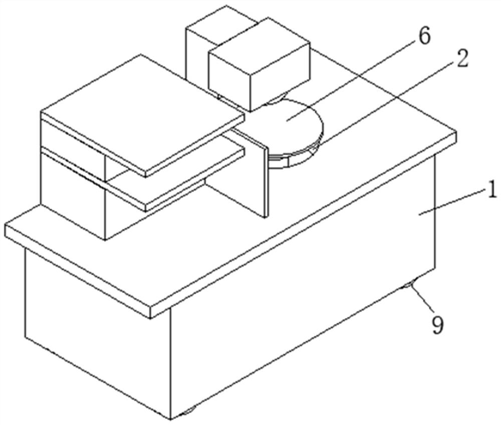
[0021] Embodiment one: refer to as figure 1 Shown: a multi-ultra-thin chip packaging equipment, including a chip processing device body 1, the four corners of the bottom of the chip processing device body 1 are fixedly connected with a base 9, the shape of the base 9 is circular, and the bottom of the base 9 is provided with anti-skid lines , through the setting of the base 9, the frictional force between the chip processing device body 1 and the ground is increased, and the stability of the chip processing device body 1 is improved. The top of the chip processing device body 1 is provided with a housing 2, and the shell The diameter of the body 2 is not less than ten centimeters, the depth of the shell 2 is not less than fifteen centimeters, and the top of the rotating plate 5 is movably connected with a processing plate 6
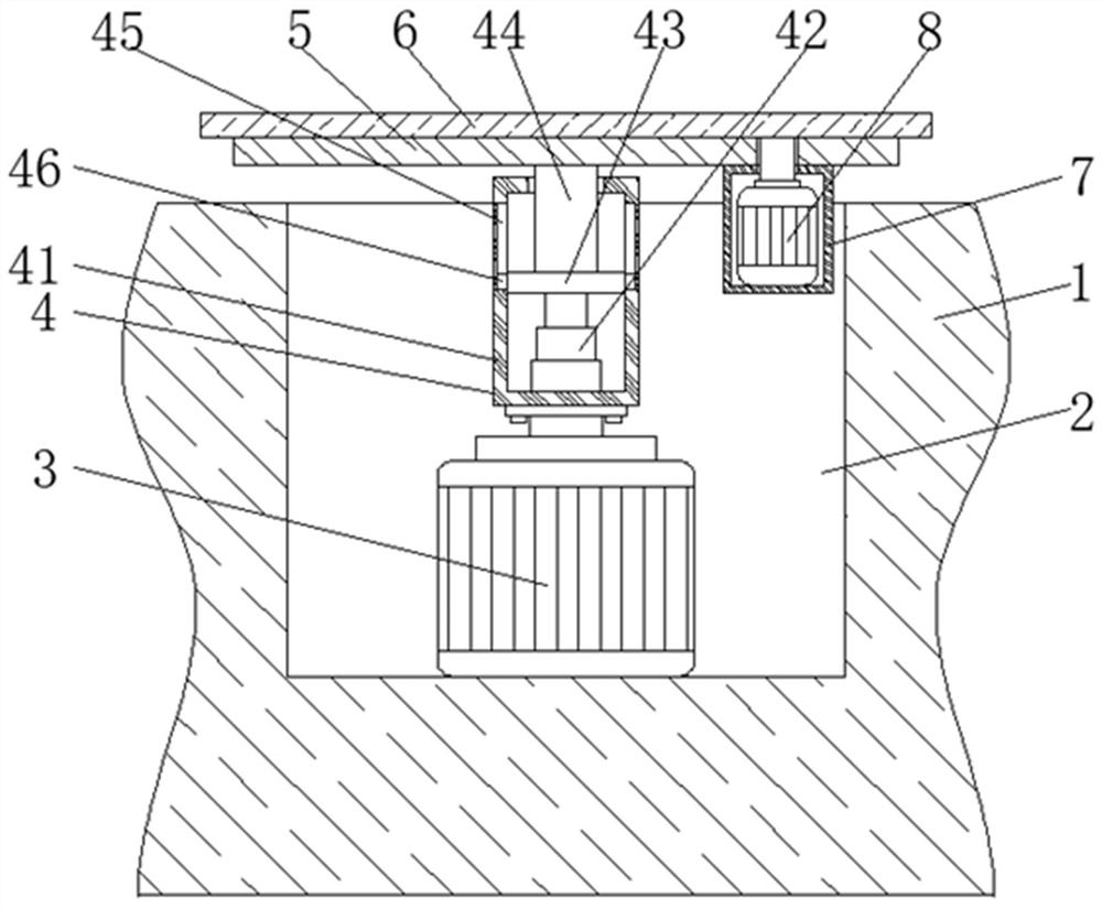
[0022] Refer to as figure 2 As shown: the bottom of the inner cavity of the housing 2 is fixedly connected with the motor one 3, and the output shaft o...
Embodiment 2
[0024]The present invention provides a technical solution: a multi-ultra-thin chip packaging equipment, including a chip processing device body 1, the four corners of the bottom of the chip processing device body 1 are fixedly connected with a base 9, the shape of the base 9 is circular, and the base 9 The bottom is provided with anti-slip lines. Through the setting of the base 9, the frictional force between the chip processing device body 1 and the ground is increased, and the stability of the chip processing device body 1 is improved. The top of the chip processing device body 1 is provided with Housing 2, the diameter of housing 2 is not less than ten centimeters, the depth of housing 2 is not less than fifteen centimeters, the bottom of the inner cavity of housing 2 is fixedly connected with motor one 3, and the output shaft of motor one 3 is fixedly connected with a lifting structure 4. The top of the lifting structure 4 penetrates into the inner cavity of the chip proces...
Embodiment 3
[0026] The present invention provides a technical solution: a multi-ultra-thin chip packaging equipment, including a chip processing device body 1, a housing 2 is arranged on the top of the chip processing device body 1, and a motor 3 is welded on the bottom of the inner cavity of the housing 2, The output shaft of the motor one 3 is welded with a lifting structure 4, the top of the lifting structure 4 penetrates into the inner cavity of the chip processing device body 1 and is welded with a rotating plate 5, the top of the rotating plate 5 is movably connected with a processing plate 6, and the bottom of the rotating plate 5 The left side of the motor box 7 is welded with a motor box 7, and the bottom of the motor box 7 inner cavity is welded with a motor two 8, and the output shaft of the motor two 8 runs through to the top of the rotating plate 5 and is welded with the processing plate 6.
[0027] In the present invention: the lifting structure 4 includes a fixed pipe 41 wel...
PUM
 Abstract
Description
Claims
Application Information
 - R&D Engineer
- R&D Manager
- IP Professional
- Industry Leading Data Capabilities
- Powerful AI technology
- Patent DNA Extraction
Browse by: Latest US Patents, China's latest patents, Technical Efficacy Thesaurus, Application Domain, Technology Topic, Popular Technical Reports.
© 2024 PatSnap. All rights reserved.Legal|Privacy policy|Modern Slavery Act Transparency Statement|Sitemap|About US| Contact US: help@patsnap.com