


Quick Research
Generate reliable direction feasibility study reports for your R&D in just a few steps.

Technical Q&A
Discover and master advanced knowledge NOW. Basics, ideas, possibilities, all at once.

Find Solutions
As an expert in R&D theories, this can generate solutions to your technical problems instantly.

Evaluate Feasibility
Analyze your overall solution with one click, know your potential R&D risks in advance.

Monitor Landscape
Get weekly tech updates, stay abreast of the latest tech innovations and key insights.
Planar optical waveguide chip and waveguide type single-mode fiber laser
A planar optical waveguide and laser technology, applied in the field of lasers, can solve the problems of irregular beam space derivation, small optical parameter product, difficult integration and beam expansion, etc.
- Summary
- Abstract
- Description
- Claims
- Application Information
AI Technical Summary
Problems solved by technology
Method used
Image

Examples
Embodiment 1
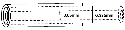
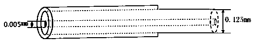
[0030] Such as Figure 1-Figure 5 , Figure 7 As shown, a planar optical waveguide chip provided by the present invention includes a planar optical waveguide chip main body 1. The planar optical waveguide chip main body 1 is used for docking and coupling the laser light emitted by the semiconductor laser 2. The planar optical waveguide chip main body 1 includes an optical input terminal 11 and the light output end 10, from the light input end 11 to the light output end 10, the waveguide width 12 decreases gradually.
[0031] Specifically, from the light incident end 11 to the light exit end 10, the thickness 13 of the waveguide remains unchanged.
[0032] Specifically, the waveguide thickness 13 and the waveguide width 12 of the light output end 10 are equal.
[0033] Specifically, the light incident end 11 is a long rectangle slightly larger than the emission area 27 of the surface 28 of the semiconductor light-emitting cavity.
[0034] Specifically, the laser light is dif...
Embodiment 2
[0049] Such as Figure 1-7 As shown, 976nm single-mode fiber laser production:
[0050] semiconductor laser light source Figure 5 Preparation: This semiconductor laser light source is purchased from a domestic research institute. It is a semiconductor light source device with relatively high output power in China: the light-emitting wavelength is 976nm, the output power of a single tube is 10W, and the length of the slow axis of the light-emitting end face, that is, the width of the light-emitting area, is 90 microns. The length of the fast axis is 1 micron, which is the height of the light-emitting area;
[0051] planar waveguide chip Figure 4 Preparation: The planar optical waveguide chip is made of quartz glass, and the specific manufacturing process is the current popular semiconductor photolithography process. The width of the light-incoming end of the planar optical waveguide chip is 100 microns, the thickness of the waveguide is 3 microns and remains constant every...
PUM
| Property | Measurement | Unit |
|---|---|---|
| width | aaaaa | aaaaa |
| width | aaaaa | aaaaa |
| emission peak | aaaaa | aaaaa |
Abstract
Description
Claims
Application Information
 - R&D Engineer
- R&D Manager
- IP Professional
- Industry Leading Data Capabilities
- Powerful AI technology
- Patent DNA Extraction
Browse by: Latest US Patents, China's latest patents, Technical Efficacy Thesaurus, Application Domain, Technology Topic, Popular Technical Reports.
© 2024 PatSnap. All rights reserved.Legal|Privacy policy|Modern Slavery Act Transparency Statement|Sitemap|About US| Contact US: help@patsnap.com