Photomask structure
A photomask and pattern technology, applied in optics, originals for opto-mechanical processing, instruments, etc., can solve the problems of a large number of photomasks and high production costs
- Summary
- Abstract
- Description
- Claims
- Application Information
AI Technical Summary
Problems solved by technology
Method used
Image
Examples
Embodiment Construction
[0061] In order to more clearly illustrate the technical solutions in the embodiments or the prior art, the accompanying drawings that need to be used in the description of the embodiments or the prior art will be briefly introduced below. Obviously, the accompanying drawings in the following description are only for invention For some embodiments, those of ordinary skill in the art can also obtain other drawings based on these drawings without any creative effort.
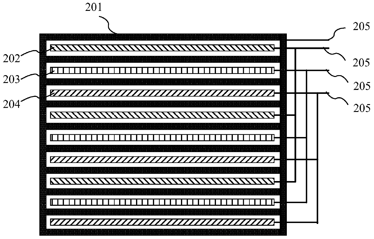
[0062] Specifically, see figure 1 , which is a cross-sectional view of a photomask structure provided by an embodiment of the present application, including: a transparent substrate 101 ; and a photomask pattern disposed on the transparent substrate 101 . Wherein, the photomask pattern at least includes: first nanomaterial patterns 103 distributed in an array, each of the first nanomaterial patterns 103 is electrically connected; a transparent insulating layer, covering at least the first nanomaterial patterns 103...
PUM
 Abstract
Description
Claims
Application Information
 - R&D
- Intellectual Property
- Life Sciences
- Materials
- Tech Scout
- Unparalleled Data Quality
- Higher Quality Content
- 60% Fewer Hallucinations
Browse by: Latest US Patents, China's latest patents, Technical Efficacy Thesaurus, Application Domain, Technology Topic, Popular Technical Reports.
© 2025 PatSnap. All rights reserved.Legal|Privacy policy|Modern Slavery Act Transparency Statement|Sitemap|About US| Contact US: help@patsnap.com


