Circuit board assembly and terminal
A circuit board assembly and circuit board technology, which is applied in the direction of printed circuit components, circuit devices, electrical components, etc., can solve the problems of limited plane area and the inability of multiple electronic components to be integrated circuit boards at the same time
- Summary
- Abstract
- Description
- Claims
- Application Information
AI Technical Summary
Problems solved by technology
Method used
Image

Examples
example 1
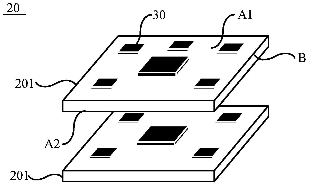
[0096] In this example, one first riser board 202 is electrically connected to the side B on the same side of at least two layers of circuit boards 201 .
[0097] For example, in some embodiments of the present application, such as Figure 4a As shown, the circuit board assembly 20 includes a circuit board 201a and a circuit board 201b.
[0098] The first riser board 202a is electrically connected to the left side B of the circuit board 201a and the left side B of the circuit board 201b. The first riser board 202b is electrically connected to the right side B of the circuit board 201a and the right side B of the circuit board 201b.
[0099] In this case, the circuit board 201a and the electronic components 30 integrated on the circuit board 201a form a first unit module. During the working process of the first unit module, the generated signal can be transmitted to the circuit board 201b through the first adapter board 202a and the first adapter board 202b. The circuit boar...
example 2
[0109] In this example, a first adapter board 202 is electrically connected to the upper surface A1 or the lower surface A2 of one layer of circuit boards 201 among at least two layers of circuit boards 201, and is connected to at least one of the remaining two layers of circuit boards 201. The side B of the layered circuit board 201 is electrically connected.
[0110] Taking the circuit board assembly 20 including a circuit board 201a, a circuit board 201b and a circuit board 201c as an example, in some embodiments of the present application, as Figure 5a As shown, the first adapter board 202a on the left side of the circuit board assembly 20 is electrically connected to the upper surface A1 of the circuit board 201a, and is electrically connected to the side B of the circuit board 201b.
[0111] In this case, the circuit board 201a and the circuit board 201b can be electrically connected through the first adapter board 202a to realize signal transmission.
[0112] In addit...
example 3
[0116] In this example, one end of a first adapter board 202 is electrically connected to the upper surface A1 of one layer of circuit boards 201 among at least two layers of circuit boards 201, and the other end is electrically connected to the remaining one layer of circuit boards in at least two layers of circuit boards 201. The lower surface A2 of 201 is electrically connected.
[0117] In some embodiments of the present application, take the circuit board assembly 20 including a circuit board 201a and a circuit board 201b as an example, such as Figure 6a As shown, the first riser board 202a on the left is electrically connected to the upper surface A1 of the circuit board 201a and the lower surface A2 of the circuit board 201b. The setting method of the first adapter plate 202b on the right is the same as that of the first adapter plate 202b.
[0118] In this case, the circuit board 201a and the circuit board 201b implement signal transmission through the first adapter ...
PUM
 Abstract
Description
Claims
Application Information
 - Generate Ideas
- Intellectual Property
- Life Sciences
- Materials
- Tech Scout
- Unparalleled Data Quality
- Higher Quality Content
- 60% Fewer Hallucinations
Browse by: Latest US Patents, China's latest patents, Technical Efficacy Thesaurus, Application Domain, Technology Topic, Popular Technical Reports.
© 2025 PatSnap. All rights reserved.Legal|Privacy policy|Modern Slavery Act Transparency Statement|Sitemap|About US| Contact US: help@patsnap.com