A polarizing multilayer film for 70-100nm vacuum ultraviolet band and its preparation method
A vacuum ultraviolet, multi-layer film technology, applied in polarizing elements, vacuum evaporation plating, coating, etc., can solve the problem of low flux of polarizing elements
- Summary
- Abstract
- Description
- Claims
- Application Information
AI Technical Summary
Problems solved by technology
Method used
Image
Examples
preparation example Construction
[0042] The present invention also provides the preparation method of the polarizing multilayer film described in the above technical scheme, comprising the following steps:
[0043] On the surface of the substrate, the first Si layer, the first Al layer, the first MgF 2 layer, second Si layer, second Al layer, second MgF 2 layer, the third Si layer, the third Al layer and the third MgF 2 Layer magnetron sputtering.
[0044] The present invention has no special limitation on the material of the substrate.
[0045]In the present invention, the background vacuum of the magnetron sputtering is preferably greater than 9E-5Pa; the working gas of the magnetron sputtering is preferably Ar, the flow rate of the Ar is preferably 20 sccm, and the pressure of the Ar is preferably 0.25Pa .
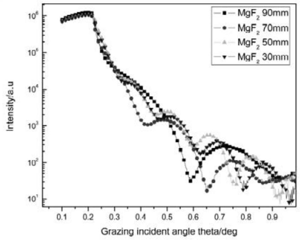
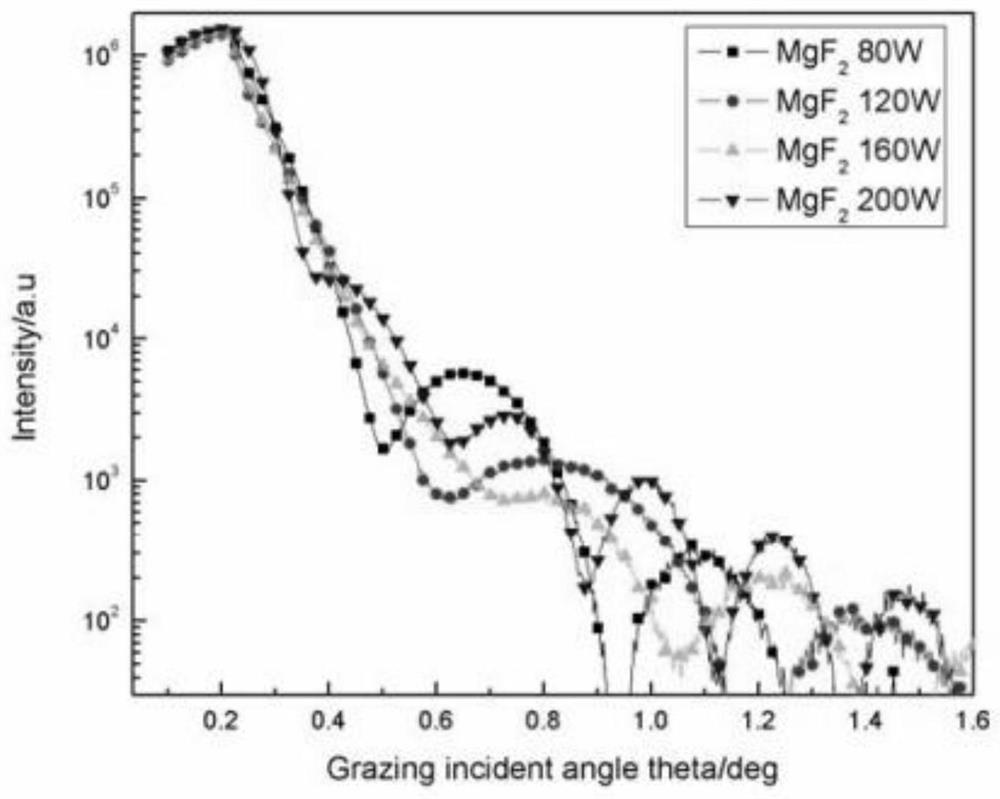
[0046] In the present invention, sputtering the first MgF 2 layer, the second MgF 2 layer and the third MgF 2 The method of layering is radio frequency magnetron sputtering, the sputtering power...
Embodiment 1
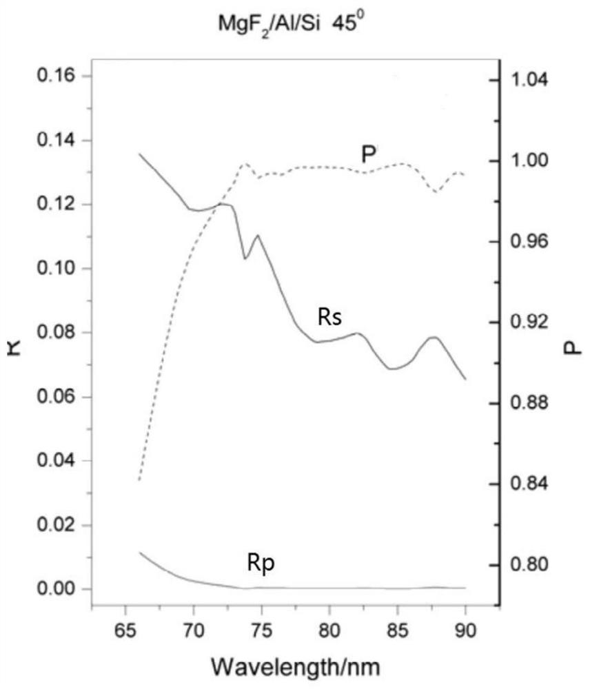
[0051] A polarizing multilayer film for the 70-100nm vacuum ultraviolet band, comprising a first Si layer, a first Al layer, and a first MgF layer stacked on the surface of a substrate in sequence 2 layer, second Si layer, second Al layer, second MgF 2 layer, the third Si layer, the third Al layer and the third MgF 2 layer, the wavelength of the vacuum ultraviolet band is 70-90nm, when the light of the vacuum ultraviolet band is incident at 45°, the thickness of the first Si layer is 15.4nm, and the thickness of the first Al layer is 2.48nm , the first MgF 2 The thickness of the layer is 2.48nm, the thickness of the second Si layer is 0.5nm, the thickness of the second Al layer is 5.44nm, the second MgF 2 layer thickness is 7.57nm, the thickness of the third Si layer is 4.7nm, the thickness of the third Al layer is 0.5nm, the third MgF 2 The thickness of the layer is 5 nm.
[0052] figure 1 R under the 45° incident angle of the polarizing multilayer film provided by Examp...
Embodiment 2
[0074] A polarizing multilayer film for the 70-100nm vacuum ultraviolet band, comprising a first Si layer, a first Al layer, and a first MgF layer stacked on the surface of a substrate in sequence 2 layer, second Si layer, second Al layer, second MgF 2 layer, the third Si layer, the third Al layer and the third MgF 2 layer, the wavelength of the vacuum ultraviolet band is 70-90nm, when the light of the vacuum ultraviolet band is incident at 60°, the thickness of the first Si layer is 20nm, and the thickness of the first Al layer is 2nm, so the first MgF 2 The thickness of the layer is 0.5nm, the thickness of the second Si layer is 30nm, the thickness of the second Al layer is 30nm, the second MgF 2 The thickness of the layer is 7.7nm, the thickness of the third Si layer is 1.8nm, the thickness of the third Al layer is 0.5nm, the third MgF 2 The thickness of the layer was 6.32 nm.
[0075] The preparation method is the same as in Example 1.
[0076] Figure 6 R under the ...
PUM
| Property | Measurement | Unit |
|---|---|---|
| thickness | aaaaa | aaaaa |
| thickness | aaaaa | aaaaa |
| thickness | aaaaa | aaaaa |
Abstract
Description
Claims
Application Information
 - R&D
- Intellectual Property
- Life Sciences
- Materials
- Tech Scout
- Unparalleled Data Quality
- Higher Quality Content
- 60% Fewer Hallucinations
Browse by: Latest US Patents, China's latest patents, Technical Efficacy Thesaurus, Application Domain, Technology Topic, Popular Technical Reports.
© 2025 PatSnap. All rights reserved.Legal|Privacy policy|Modern Slavery Act Transparency Statement|Sitemap|About US| Contact US: help@patsnap.com


