Light emitting device and display apparatusdevice

A technology of light-emitting device and light-emitting layer, which is applied in the field of light-emitting and display, can solve the problems of restricting the application of OLED, poor life and luminous efficiency, and achieve the effect of prolonging life and improving luminous efficiency

Active Publication Date: 2020-07-17
JITRI INST OF ORGANIC OPTOELECTRONICS CO LTD
View PDF2 Cites 0 Cited by
  • Summary
  • Abstract
  • Description
  • Claims
  • Application Information

AI Technical Summary

Problems solved by technology

However, due to the poor lifespan and luminous efficiency of blue light-emitting devices, the lag in the developm...

Method used


Image

  • Light emitting device and display apparatusdevice
  • Light emitting device and display apparatusdevice
  • Light emitting device and display apparatusdevice

Examples


Embodiment Construction

[0037] The present invention will be further described in detail below in conjunction with the accompanying drawings and embodiments. It should be understood that the specific embodiments described here are only used to explain the present invention, but not to limit the present invention. In addition, it should be noted that, for the convenience of description, only some structures related to the present invention are shown in the drawings but not all structures.

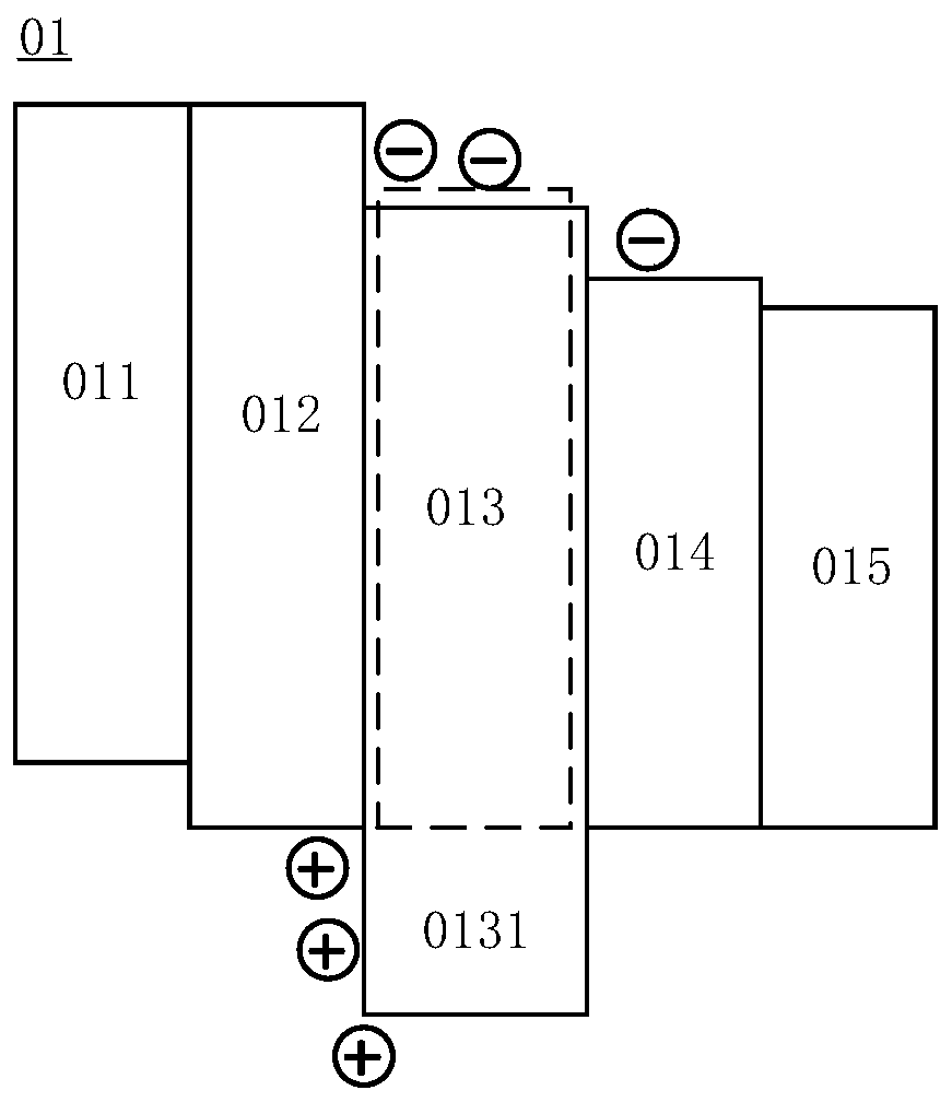
[0038] figure 1 It is a structural schematic diagram of a light-emitting device in the related art. refer to figure 1 , the light emitting device 01 includes a hole injection layer 011 , a hole transport layer 012 , a light emitting layer 013 , an electron transport layer 014 and an electron injection layer 015 stacked in sequence; wherein the light emitting layer 013 includes an electron host 0131 . That is, in the light-emitting device 01, the light-emitting guest is generally doped in an electron-type host, t...


PUM


Abstract

The embodiment of the invention discloses a light emitting device and a display device. The light emitting device includes a first electrode layer; the a second electrode layer which is arranged opposite to the first electrode layer; a hole transport layer disposed which is arranged between the first electrode layer and the second electrode layer; and a light emitting layer disposed which is arranged between the hole transport layer and the second electrode layer,; wherein the light -emitting layer comprises a first sub-light -emitting layer and a second sub-light -emitting layer, and the first sub-light -emitting layer is located on the side, facing the hole transport layer, of the second sub-light -emitting layer; wherein the first sub-light -emitting layer comprises a first hole type host material, a first electronic type host material and a first object material; the second sub-light -emitting layer comprises a second electronic type host material and a second object material; thelight -emitting color of the second object material is the same as the light -emitting color of the first object material. Therefore, the recombination region of excitons is broadened; meanwhile, theproblems of quenching effect and color purity caused by continuous transmission of holes to the second electrode layer are avoided, and the service life of the light -emitting device is prolonged while the light -emitting efficiency of the light -emitting device is improved.

Description

technical field [0001] The invention relates to the technical field of light emitting and display, in particular to a light emitting device and a display device. Background technique [0002] With the development of display technology, organic light emitting diode (Organic Light Emitting Diode, OLED) display panel gradually enters the market, compared with traditional thin film transistor liquid crystal display panel (Thin Film Transistor Liquid Crystal Display, TFT LCD), OLED display panel has performance It has the advantages of low power consumption, self-illumination, wide viewing angle, fast response speed and easy application to flexible display technology. [0003] Generally, no matter in the field of OLED display or lighting, whether it is using the three primary colors of red, green and blue, or orange light and blue light complementary to achieve full-color technology, the blue light component is essential. However, due to the poor lifespan and luminous efficiency...

Claims


Application Information

Patent Timeline
IPC IPC(8): H01L51/50H01L27/32
CPCH10K59/00H10K50/11H10K2101/40H10K50/121
Inventor 朱凯祝晓钊王浩王波何欢欢冯敏强廖良生
Owner JITRI INST OF ORGANIC OPTOELECTRONICS CO LTD
Why Eureka
Try Eureka