
A crucible for silicon carbide single crystal growth, growth method and growth device

A silicon carbide single crystal, silicon carbide technology, applied in the direction of single crystal growth, single crystal growth, crystal growth, etc., can solve the problems of uneven heating, rough crucible structure, etc., to improve efficiency, reduce inclusions, temperature The effect of field distribution averaging

Active Publication Date: 2021-02-12
CEC COMPOUND SEMICON CO LTD
View PDF4 Cites 0 Cited by
  • Summary
  • Abstract
  • Description
  • Claims
  • Application Information

AI Technical Summary

Problems solved by technology

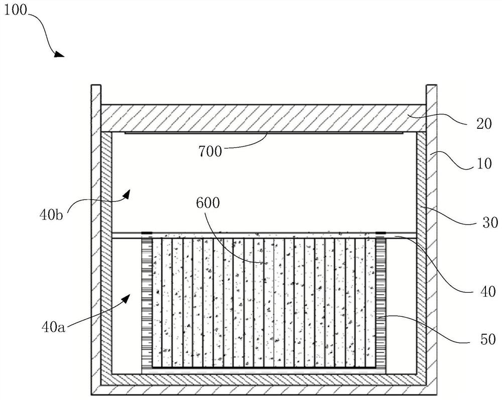
[0004] In view of the shortcomings of the prior art described above, one of the objectives of the present invention is to provide a crucible for SiC single crystal growth, which can improve and optimize the temperature inside the growth chamber by changing the structure of the inner chamber and the charging method. Field distribution, through the dual scheme of blocking and optimizing the temperature field distribution to reduce the impurity inclusions in the growth of SiC single crystal, it is used to solve the problem of rough crucible structure and uneven heating of SiC single crystal in the prior art, which causes the sintering of raw materials into agglomerates And the problem of excessive carbonization affecting the quality of SiC single crystal growth

Method used


Image

  • A crucible for silicon carbide single crystal growth, growth method and growth device
  • A crucible for silicon carbide single crystal growth, growth method and growth device
  • A crucible for silicon carbide single crystal growth, growth method and growth device

Examples


Embodiment Construction

[0023] The present invention will be further described by several specific examples below, but it should be pointed out that the specific material proportions, process conditions and results described in the examples of the present invention are only used to illustrate the present invention, and cannot be used as This limits the protection scope of the present invention, and all equivalent changes or modifications made according to the spirit of the present invention shall fall within the protection scope of the present invention. Note that "%" shown in the description herein refers to "parts by mass" unless otherwise specified.

[0024] As used herein, the singular forms "a", "an" and "the" include plural forms unless the context clearly dictates otherwise. Thus, for example, when "a compound" is mentioned, it includes a plurality of such compounds, and when "a component" or "an additive" is mentioned, it means that one or more Components or additives and their equivalents k...


PUM

PropertyMeasurementUnit
electrical resistivityaaaaaaaaaa
heightaaaaaaaaaa
diameteraaaaaaaaaa

Abstract

The invention discloses a crucible for growing a silicon carbide single crystal, a growing method and a growing device. The crucible for growing the silicon carbide single crystal comprises a first crucible main body, a first cover body, a second crucible main body, a second cover body and a raw material accommodating part; the first cover body is arranged on the first crucible main body; the second crucible main body is arranged in the first crucible main body, and an accommodating cavity is formed by the second crucible main body and the first cover body; the second cover body is located inthe accommodating cavity, and the accommodating cavity is divided into a raw material cavity and a growth cavity which are oppositely arranged; the raw material accommodating part is positioned in theraw material cavity; the porosity among the second crucible main body, the second cover body and the raw material accommodating part is different. The crucible for silicon carbide single crystal growth provided by the invention is a favorable tool for designing and optimizing the temperature field, and can effectively improve and optimize the temperature field distribution in the growth chamber and improve the quality of the silicon carbide single crystal.

Description

technical field [0001] The invention belongs to the technical field of semiconductor material manufacturing, and in particular relates to a crucible for growing a silicon carbide single crystal, a growth method and a growth device. Background technique [0002] Silicon carbide (SiC) material can be used for high temperature resistance, High-frequency, radiation-resistant, and high-power semiconductor device materials have broad application prospects. However, due to the harsh growth conditions of SiC single crystals, they are easily affected by the environment, resulting in product quality defects. For the excellent performance of the device, its growth technology is the key. [0003] At present, the current crystal growth equipment for growing SiC by PVT method adopts the medium frequency induction heating method, and the magnetic field generated by the medium frequency coil acts on the graphite crucible for heating, so that the internal SiC raw material is sublimated, and...

Claims


Application Information

Patent Timeline
Patent Type & Authority Patents(China)
IPC IPC(8): C30B29/36C30B23/00
CPCC30B23/00C30B29/36
Inventor 周玉洁马远潘尧波
Owner CEC COMPOUND SEMICON CO LTD
Learn More