Packaging structure and manufacturing method thereof

A technology of packaging structure and manufacturing method, which is applied in semiconductor/solid-state device manufacturing, electrical components, electric solid-state devices, etc., can solve the problems of poor heat dissipation performance, poor heat dissipation performance, and unsafety of packaging structures, so as to reduce the expansion coefficient and improve Effect of heat dissipation performance and safety improvement

Active Publication Date: 2020-06-30
GREE ELECTRIC APPLIANCES INC +1
View PDF4 Cites 0 Cited by
  • Summary
  • Abstract
  • Description
  • Claims
  • Application Information

AI Technical Summary

Problems solved by technology

[0006] In view of the disadvantages of poor heat dissipation performance of the packaging structure in the prior art, easy to break free from leads, and poor fixation and unsafe testing, the purpose of the present invention is to provide a packaging structure, which can effectively solve the problem of poor heat dissipation performance of the existing packaging structure, easy Unsafe problems of loose leads and poor fixation

Method used


Image

  • Packaging structure and manufacturing method thereof
  • Packaging structure and manufacturing method thereof
  • Packaging structure and manufacturing method thereof

Examples


Embodiment 1

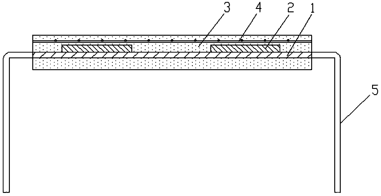
[0039] The packaging structure provided in this embodiment includes a heat-conducting bottom sheet 1 , a chip 2 , a molding material layer 3 and a heat-conducting net 4 . Wherein, the chip 2 is fixed on the heat conduction base 1 , and the connection point on the chip 2 is electrically connected to the pin 5 on the heat conduction base 1 . The heat conduction net 4 wraps the chip 2 and is not in contact with the chip 2, that is, the heat conduction net 4 is suspended above the chip 2. This packaging structure is not only suitable for the heat conduction net 4 made of non-conductive heat conduction material, but also especially suitable for The heat conduction mesh 4 (such as metal mesh) made of conductive heat conduction material will not cause a short circuit because the heat conduction mesh 4 is not in direct contact with the chip 2 . There are two ways to suspend the heat conduction net 4 above the chip 2: the first method is to use multiple fixing frames to fix the heat co...

Embodiment 2

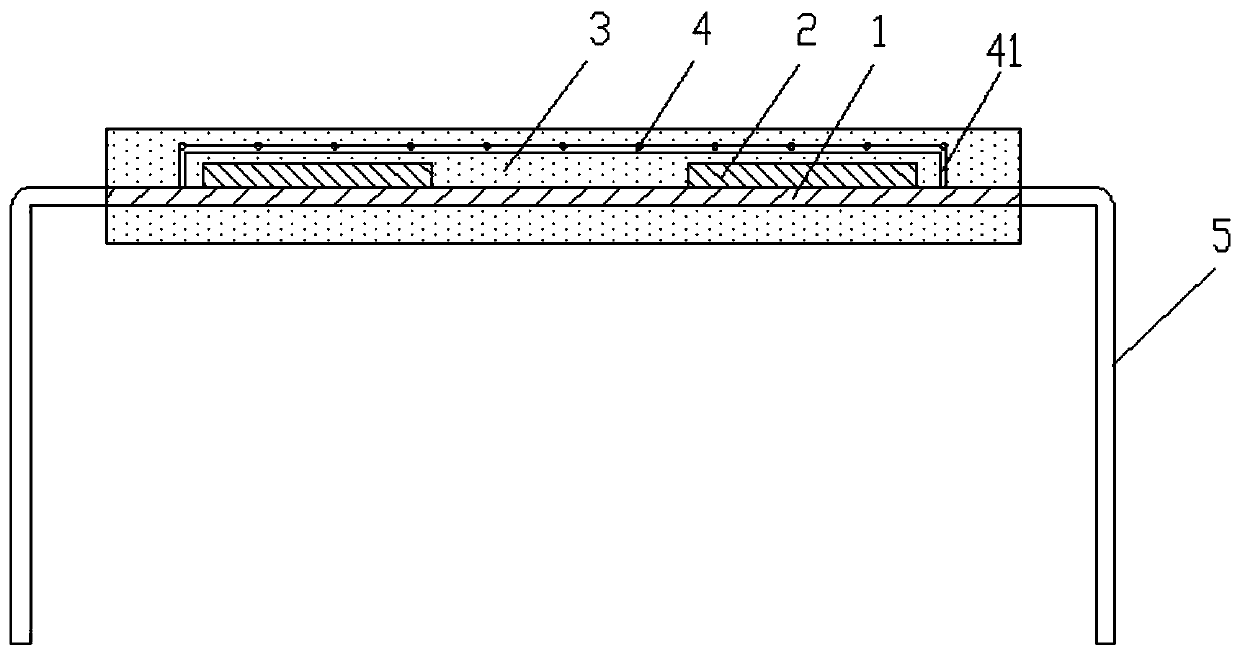
[0041] Such as Figure 4 As shown, the packaging structure provided in this embodiment includes a heat-conducting backsheet 1 , a chip 2 , a molding material layer 3 and a heat-conducting net 4 . Wherein, the chip 2 is fixed on the heat conduction base 1 , and the connection point on the chip 2 is electrically connected to the pin 5 on the heat conduction base 1 . The heat conduction net 4 wraps the chip 2 and is in contact with the chip 2, that is, the heat conduction net 4 is placed on the chip 2. This packaging structure has a simple structure of the heat conduction net 4 and only needs to place the heat conduction net 4 on the chip 2 before injection molding. That is, there is no need to add other fixing or supporting devices and steps, and the operation is simple. However, since the heat conduction net 4 is in direct contact with the chip 2, this packaging structure is only suitable for the case where the heat conduction net 4 is made of non-conductive heat conduction mat...


PUM


Abstract

The invention provides a packaging structure and a manufacturing method thereof, the packaging structure comprises a heat conduction bottom sheet, a chip, pins and a plastic packaging material layer;the chip is fixed on the heat conduction bottom sheet, the chip is electrically connected with the pins, the packaging structure also comprises a heat conduction net, the heat conduction net wraps thechip, and the heat conduction net is embedded in the plastic packaging material layer. According to the packaging structure provided by the invention, the heat conduction net is embedded in the plastic packaging material layer, so that the heat dissipation performance of the packaging structure is improved, and the problem that heat around a chip cannot be dissipated in time due to poor heat dissipation of a plastic packaging material in an existing packaging structure is effectively solved; uniform heating of an injection molding material is facilitated, and the expansion coefficient of theinjection molding material is reduced, so that the problem that leads are easy to break away due to non-uniform injection molding heating in an existing packaging structure is effectively solved; besides, when accidental explosion occurs, the chip is wrapped by the heat conduction net so that the chip is enabled not to bounce off the shell, and thus safety of the packaging structure can be enhanced.

Description

technical field [0001] The invention relates to the technical field of module packaging, in particular to a packaging structure and a manufacturing method thereof. Background technique [0002] At present, the packaging of the intelligent power module (IPM) module is basically to fix the chip on the heat-dissipating copper sheet first, and then inject the plastic packaging material (such as gel-like material) into the packaging. This packaging structure has the following problems: [0003] 1. The heat dissipation of the plastic packaging material is not good, and the heat around the chip cannot be dissipated in time; [0004] 2. The plastic sealing material is heated unevenly, and it is easy to break away from the lead wire; [0005] 3. The fixation is not good. When the chip explodes during the test phase, the plastic packaging material will be blown away, so the test is not safe. Contents of the invention [0006] In view of the disadvantages of poor heat dissipation p...

Claims


Application Information

Patent Timeline
Patent Type & Authority Applications(China)
IPC IPC(8): H01L23/373H01L23/31H01L23/00H01L21/56
CPCH01L23/3733H01L23/3736H01L23/564H01L23/3114H01L21/56
Inventor 林志龙敖利波史波曾丹
Owner GREE ELECTRIC APPLIANCES INC
Why Eureka
Try Eureka